ISL97675IRZ-TK Intersil, ISL97675IRZ-TK Datasheet
ISL97675IRZ-TK
Specifications of ISL97675IRZ-TK


Related parts for ISL97675IRZ-TK

ISL97675IRZ-TK Summary of contents
Page 1
... AGND * V 9 AGND CAUTION: These devices are sensitive to electrostatic discharge; follow proper IC Handling Procedures. | 1-888-INTERSIL or 1-888-468-3774 Intersil (and design registered trademark of Intersil Americas Inc. All other trademarks mentioned are the property of their respective owners. Short Circuit OUT (see page 19 45V max* ...
Page 2
Block Diagram VIN* = 4.5V~26V VIN EN 4.75V BIAS REG VDDIO OSC & RAMP COMP FSW/ PHASE PHASESHIFT SELECT FSW DETECT COMP + - ISET REF OVP REF VSC GND PHASE SELECT PWM 8-BIT DIGITIZER FPWM/DirectPWM DIRECTPWM DETECT OPTIONAL PFET ...
Page 3
Pin Configuration FSW/PhaseShift Pin Descriptions (I = Input Output Supply) PIN NAME PIN NO. TYPE VDDIO FSW/PhaseShift 3 ISET FB4 6 FB3 7 AGND 8, 9 FB2 11 FB1 ...
Page 4
... EP 21 Ordering Information PART NUMBER (Notes MARKING ISL97675IRZ 976 75IRZ NOTES: 1. Please refer to TB347 for details on reel specifications. 2. These Intersil Pb-free plastic packaged products employ special Pb-free material sets, molding compounds/die attach materials, and 100% matte tin plate plus anneal (e3 termination finish, which is RoHS compliant and compatible with both SnPb and Pb-free soldering operations) ...
Page 5
Table of Contents Typical Application Circuit ................................................................................................................... 1 Block Diagram ..................................................................................................................................... 2 Pin Descriptions (I = Input Output Supply) .......................................................................... 3 Absolute Maximum Ratings ................................................................................................................. 6 Thermal Information ........................................................................................................................... 6 Operating Conditions ........................................................................................................................... 6 Electrical Specifications ...
Page 6
... Thermal Resistance (Typical QFN Package (Notes Thermal Characterization (Typical QFN Package (Note Maximum Continuous Junction Temperature . . . . . . +125°C Storage Temperature . . . . . . . . . . . . . . . -65°C to +150°C Pb-free reflow profile . . . . . . . . . . . . . . . . . . .see link below http://www.intersil.com/pbfree/Pb-FreeReflow.asp Operating Conditions Temperature Range . . . . . . . . . . . . . . . . . . -40°C to +85°C A CONDITION 4.5V < V ≤ 26V, ...
Page 7
Electrical Specifications All specifications below are tested at T unless otherwise noted. Boldface limits apply over the operating temperature range, -40°C to +85°C. (Continued) SYMBOL PARAMETER BOOST SWILimit Boost FET Current Limit r Internal Boost Switch ON-Resistance DS(ON) SS Soft-Start ...
Page 8
Electrical Specifications All specifications below are tested at T unless otherwise noted. Boldface limits apply over the operating temperature range, -40°C to +85°C. (Continued) SYMBOL PARAMETER FAULT DETECTION V Channel Short Circuit Threshold SC V Over-Temperature Threshold Accuracy TEMP_ACC V ...
Page 9
Typical Performance Curves 100 80 12V (mA) LED FIGURE 1. EFFICIENCY vs 20mA LED CURRENT (100% LED DUTY CYCLE) for 4P12S vs V 100 80 20mA/582kHz ...
Page 10
Typical Performance Curves 1.0 0.8 0.6 12V 0.4 0 (%) FIGURE 7. CURRENT LINEARITY vs LOW LEVEL PWM DIMMING DUTY CYCLE vs V 0.60 +25°C 0.55 0.50 0°C 0.45 0. ...
Page 11
Typical Performance Curves FIGURE 13. LINE REGULATION WITH V FROM 6V TO 26V 20mA/CHANNEL FIGURE 15. LOAD REGULATION WITH I FROM 0% TO 100% PWM DIMMING 12V, 4P12S AT 20mA/CHANNEL IN FIGURE 17. ISL97675 SHUTS DOWN ...
Page 12
Theory of Operation PWM Boost Converter The current mode PWM boost converter produces the minimal voltage needed to enable the LED stack with the highest forward voltage drop to run at the programmed current. The ISL97675 employs current mode control ...
Page 13
For example, if the maximum required LED current ( 20mA, rearranging Equation 3 yields LED(max) Equation 0.02 ⁄ R 392 19.6kΩ ISET PWM Control The ISL97675 has a high speed 8-bit digitizer that ...
Page 14
Equation 6 and Equation 7 can only be integer because the PWM dimming is controlled by an internal 8-bit digital counter result, any decimal value of (255/N) will be discarded. For example for N = ...
Page 15
For systems with no master fault protection FET, the inrush current will flow towards C OUT and it is determined by the ramp rate of V values of C and boost inductor, L. OUT Fault Protection and Monitoring The ISL97675 ...
Page 16
The upper threshold is set to +150°C. Each time this is reached, the boost will stop switching and the output current sources will be switched off ...
Page 17
CASE FAILURE MODE DETECTION MODE 5 FB1 LED Open Upper OTP not triggered Circuit but has and FB1 < 4V paralleled Zener 6 FB1 LED Open Upper OTP triggered but Circuit but has FB1 < 4V paralleled Zener 7 FB1 ...
Page 18
Inductor The selection of the inductor should be based on its maximum current (I ) characteristics, power SAT dissipation (DCR), EMI susceptibility (shielded vs unshielded), and size. Inductor type and value influence many key parameters, including ripple current, current limit, ...
Page 19
... Accordingly, the reader is cautioned to verify that data sheets are current before placing orders. Information furnished by Intersil is believed to be accurate and reliable. However, no responsibility is assumed by Intersil or its subsidiaries for its use; nor for any infringements of patents or other rights of third parties which may result from its use. No license is granted by implication or otherwise under any patent or patent rights of Intersil or its subsidiaries ...
Page 20
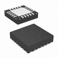
Package Outline Drawing L20.4x4C 20 LEAD QUAD FLAT NO-LEAD PLASTIC PACKAGE Rev 0, 11/06 4.00 6 PIN 1 INDEX AREA (4X) 0.15 TOP VIEW ( 3. 8 TYP ) ( TYPICAL RECOMMENDED LAND PATTERN 20 ISL97675 16X ...