IR2D07 Sharp Microelectronics, IR2D07 Datasheet - Page 10
IR2D07
Manufacturer Part Number
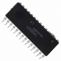
IR2D07
Description
IC LED DRIVER LINEAR 28-SDIP
Manufacturer
Sharp Microelectronics
Type
Linear (Non-Switching)r
Datasheet
1.IR2D07.pdf
(21 pages)
Specifications of IR2D07
Constant Current
Yes
Number Of Outputs
16
Internal Driver
Yes
Type - Primary
General Purpose
Frequency
20MHz
Voltage - Supply
3 V ~ 5.5 V
Voltage - Output
3V
Mounting Type
Through Hole
Package / Case
28-SDIP (0.400", 10.16mm)
Operating Temperature
-40°C ~ 100°C
Current - Output / Channel
48.5mA
Internal Switch(s)
Yes
Low Level Output Current
1 mA
High Level Output Current
- 1 mA
Operating Supply Voltage
3 V to 5.5 V
Maximum Supply Current
1.5 mA
Maximum Power Dissipation
1350 mW
Maximum Operating Temperature
+ 100 C
Mounting Style
Through Hole
Minimum Operating Temperature
- 40 C
Lead Free Status / RoHS Status
Lead free / RoHS Compliant
Efficiency
-
Topology
-
Lead Free Status / Rohs Status
Details
Other names
425-2711-5


10.Electrical Characteristics
10−2. Switching Characteristics
Refer to the timing chart (p10)
Note 2:
Note 1 : Data is inputted so that all output terminals may be set to "ON", and XEN terminal = "H"
CLOCK pulse width
Clock frequency
Set-up time for CLOCK terminal
Hold time for CLOCK terminal
CLK ↑ -LATCH ↓
LATCH ↑ -CLK ↑
LATCH ↓ -EN ↓
LATCH pulse width
Maximum CLK & LATCH rise time
Maximum CLK & LATCH fall time
If the device is connected in a cascade and tr/tf for the waveform is large,
it might not be able to secure the timing required for data transfer.
Please consider the timing carefully.
10―1.DC Electrical Characteristics
"H"Input voltage
"L"Input voltage
S-OUT terminal
Output voltage
Output leakage current
Output current
R-EXT terminal voltage
Input Pull-Up resistor
Supply current
Error between bits
Supply voltage regulation
Parameter
Parameter
Symbol
I
∆Vref Ta=25℃
OLEAK
IDD1
∆I
V
I
Vref
V
V
R
V
OUT
OH
OL
IH
IN
IL
OL
Symbol
PW
PW
t
t
t
f
HOLD
STUP
t
t
L-EN
CLK
C-L
L-C
tr
tf
CLK
LAT
VDD=3.3V,I
VDD=3.3V,I
VOUT=7.0V, Per one terminal.
VDD=3.3V
R-EXT resistor = 5kΩ
VOUT=0.6V
Ta=25 ℃
R-EXT resistor=5kΩ
LATCH,XEN
VDD=3.3V(Note 1)
R-EXT resistor=5kΩ, CLK=0Hz
The period VI(CLK) is "H"
The period VI(CLK) is "L"
Duty=50±10%
S-IN-CLK ↑
CLK ↑ -S-IN
CLK ↑ -LATCH ↓
LATCH ↑ -CLK ↑
LATCH ↓ -EN ↓
The period LATCH is "L"
(Note 2)
(Note 2)
IR2D07
O H
O L
=-1.0mA
=1.0mA
Conditions
Conditions
Reference
VDD=3.3V
VDD=3.0V→3.6V
( VDD=3.0 ∼ 5.5V,Ta=-40 ∼ 100 ℃)
(VDD=3.0 ∼ 5.5V,Ta=-40 ∼ 100 ℃ )
MIN.
25
25
10
40
40
40
25
5
-
-
-
0.7VDD
MIN.
GND
43.5
1.18
2.7
-10
50
-
-
-
-
TYP. MAX.
-
-
-
-
-
-
-
-
-
-
-
TYP.
48.5
1.24
110
450
3.0
0.3
1.0
10
-
-
-
500
500
20
-
-
-
-
-
-
-
-
0.3VDD
MAX. Unit
VDD
1500
53.5
1.30
200
0.6
4.0
10
30
-
MHz
Unit
ns
ns
ns
ns
ns
ns
ns
ns
ns
ns
mA
±%
mV
kΩ
µA
µA
V
V
V
9
Related parts for IR2D07
Image
Part Number
Description
Manufacturer
Datasheet
Request
R

Part Number:
Description:
IC FLASH 32MBIT 110NS 56SSOP
Manufacturer:
Sharp Microelectronics
Datasheet:

Part Number:
Description:
IC FLASH 16MBIT 100NS 56TSOP
Manufacturer:
Sharp Microelectronics
Datasheet:

Part Number:
Description:
IC FLASH 64MBIT 120NS 56TSOP
Manufacturer:
Sharp Microelectronics
Datasheet:

Part Number:
Description:
IC FLASH 16MBIT 90NS 48TSOP
Manufacturer:
Sharp Microelectronics
Datasheet:
Part Number:
Description:
IC SRAM 16KBIT 100NS 24DIP
Manufacturer:
Sharp Microelectronics
Datasheet:
Part Number:
Description:
IC SRAM 16KBIT 100NS 24SOP
Manufacturer:
Sharp Microelectronics
Datasheet:
Part Number:
Description:
IC SRAM 64KBIT 100NS 28DIP
Manufacturer:
Sharp Microelectronics
Datasheet:
Part Number:
Description:
IC SRAM 64KBIT 100NS 28SOP
Manufacturer:
Sharp Microelectronics
Datasheet:
Part Number:
Description:
IC SRAM 64KBIT 100NS 28SOP
Manufacturer:
Sharp Microelectronics
Datasheet:
Part Number:
Description:
IC SRAM 256KBIT 70NS 28DIP
Manufacturer:
Sharp Microelectronics
Datasheet:
Part Number:
Description:
IC FLASH 8MBIT 90NS 48TSOP
Manufacturer:
Sharp Microelectronics
Datasheet:
Part Number:
Description:
IC FLASH 8MBIT 85NS 40TSOP
Manufacturer:
Sharp Microelectronics
Datasheet:
Part Number:
Description:
IC FLASH 8MBIT 85NS 40TSOP
Manufacturer:
Sharp Microelectronics
Datasheet:
Part Number:
Description:
IC FLASH 16MBIT 90NS 48TSOP
Manufacturer:
Sharp Microelectronics
Datasheet:
Part Number:
Description:
IC FLASH 16MBIT 70NS 56TSOP
Manufacturer:
Sharp Microelectronics
Datasheet: