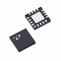
LTC5100EUF#PBF Linear Technology, LTC5100EUF#PBF Datasheet - Page 31

LTC5100EUF#PBF
Manufacturer Part Number
LTC5100EUF#PBF
Description
IC DRIVER VCSEL 3.2GBPS 16QFN
Manufacturer
Linear Technology
Type
Laser Diode Driverr
Datasheet
1.LTC5100EUF.pdf
(52 pages)
Specifications of LTC5100EUF#PBF
Data Rate
3.2Gbps
Number Of Channels
1
Voltage - Supply
3.135 V ~ 3.465 V
Current - Supply
54mA
Current - Modulation
12mA
Operating Temperature
-40°C ~ 85°C
Package / Case
16-QFN
Mounting Type
Surface Mount
Lead Free Status / RoHS Status
Lead free / RoHS Compliant
Available stocks
Company
Part Number
Manufacturer
Quantity
Price
OPERATIO
Table 3. Example of User ADC Cycle Access
ADC
CYCLE
1
2
3
4
1
2
3
4
1
2
3
4
1
2
3
4
to Use It, V1.0” by Philips Semiconductor. The 7-bit I
bus address for the LTC5100 is 0x0A (hex). When the
Read/Write bit that follows is a “1”, the resulting 8-bit word
becomes 0x15. When the Read/Write bit is a “0”, the 8-bit
word becomes 0x14. To communicate with the LTC5100,
the bus master transmits the LTC5100 address followed
by a command byte and data as defined by the I
specification and shown in Figure 28 and Table 4. Note that
16 bits of data are always transmitted, low byte first, high
byte last. Within each transmitted byte, the bit order is
SIGNAL SOURCE
T
I
I
User (V
T
I
I
User (V
T
I
I
User (V
T
I
I
User (V
M
S
M
S
M
S
M
S
TERM
LD
LD
LD
)
)
)
U
Figure 28. I
)
WRITE
READ
WRITE TO
Adc_src_sel
V
LD
S
S
2
C Serial Read/Write Sequences (LTC5100 Responses are Shown in Bold Italics)
(7 BITS) 0x0A
(7 BITS) 0x0A
ADDRESS
ADDRESS
LTC5100
LTC5100
W A
W A
READ FROM
ADC_USER
REGISTER
V
LD
COMMAND
COMMAND
BYTE
BYTE
2
C bus
A
A
S
LOW BYTE
2
C
ADDRESS
LTC5100
Adc_src
V
V
V
V
V
V
V
V
V
V
V
V
V
V
V
V
TERM
TERM
TERM
TERM
TERM
TERM
TERM
TERM
LD
LD
LD
LD
LD
LD
LD
LD
0x0A
MSB .. LSB. The register set and I
LTC5100 are documented in Table 7 through Table 30.
Table 4. Legend for the I
A HIGH BYTE A P
R
A
LOW BYTE A HIGH BYTE
Valid
0
0
0
0
1
0
0
0
1
1
0
0
1
1
1
1
SYMBOL
NA
W
R
S
A
P
Data
V
V
V
V
V
V
V
V
V
V
V
V
V
V
V
V
TERM
TERM
TERM
TERM
TERM
TERM
TERM
TERM
LD
LD
LD
LD
LD
LD
LD
LD
(1)
(1)
(1)
(1)
(2)
(2)
(2)
(2)
2
(1)
(1)
(1)
(1)
(2)
(2)
(2)
(2)
C Protocol
N
A
5100 F28
P
COMMENT
Selected Signal Source is V
ADC Updates Data with New Data,
Setting Valid
User Selects New Signal Source,
V
ADC Updates Data with New Data,
Setting Vaild and Changing Adc_src
to Reflect the Source of the New Data
User Reads the ADC_USER Register,
Clearing Valid
ADC Updates Data with New Data,
Setting Valid
LD
, Clearing Valid
2
C command set for the
No Acknowledge
Acknowledge
MEANING
LTC5100
Write
Read
Start
Stop
sn5100 5100fs
TERM
31


