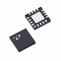
LTC5100EUF#PBF Linear Technology, LTC5100EUF#PBF Datasheet - Page 16

LTC5100EUF#PBF
Manufacturer Part Number
LTC5100EUF#PBF
Description
IC DRIVER VCSEL 3.2GBPS 16QFN
Manufacturer
Linear Technology
Type
Laser Diode Driverr
Datasheet
1.LTC5100EUF.pdf
(52 pages)
Specifications of LTC5100EUF#PBF
Data Rate
3.2Gbps
Number Of Channels
1
Voltage - Supply
3.135 V ~ 3.465 V
Current - Supply
54mA
Current - Modulation
12mA
Operating Temperature
-40°C ~ 85°C
Package / Case
16-QFN
Mounting Type
Surface Mount
Lead Free Status / RoHS Status
Lead free / RoHS Compliant
Available stocks
Company
Part Number
Manufacturer
Quantity
Price
OPERATIO
LTC5100
OVERVIEW
(Refer to Figure 1 and the Block Diagram in Figure 2)
The LTC5100 is optimized to drive common cathode
VCSELs in high speed fiber optic transceivers. The chip
incorporates several features that make it very compact
and easy-to-use while delivering exceptional high speed
performance. Only a capacitor, a resistor and a small
EEPROM (excluding laser diode and power supply filter-
ing) are needed to build a complete fiber optic transmitter.
Digital control over the I
automated laser setup to improve manufacturing effi-
ciency. The LTC5100’s extensive set of eye safety features
meet GBIC and SFF requirements but go beyond the
standards with open-pin protection, redundant transmit-
ter enable controls and other interlocks.
10-bit integrated DACs set laser bias and modulation
levels, eliminating the cost and space of digital potentiom-
eters. A multiplexed ADC allows monitoring of tempera-
ture and laser operating conditions in production or field
operation. Laser bias and modulation currents are digi-
tally temperature compensated to second order for tight
control of average power and extinction ratio. The LTC5100
16
EQUIVALE T I PUT A D OUTPUT CIRCUITS
2
3
LTC5100
Figure 10. Equivalent Circuit for the IN
IN
IN
+
–
50
50
V
V
DD(HS)
DD(HS)
U U
U
R
ON
3
2
C serial interface allows fully
20pF
25k
Cml_en
U
+
and IN
50k
50k
V
DD(HS)
–
TO INPUT
AMPLIFIER
Pins
5100 F10
provides both constant current and automatic power
control of the laser bias current. In automatic power
control mode, special circuitry maintains constant set-
tling time in spite of variations in the laser slope efficiency
and monitor diode response characteristics.
The high speed inputs of the LTC5100 are internally
terminated in 50 and internally AC coupled, eliminating
all external components at the inputs. The modulation
output is DC coupled to the laser and presents a high
quality resistive drive impedance to deliver very fast and
clean eye diagrams in spite of laser impedance variations.
The modulation output is capable of driving significant
lengths of transmission line, allowing the LTC5100 to be
placed at an arbitrary distance from the laser. This feature
allows for packaging flexibility within the module.
The LTC5100 minimizes electromagnetic interference (EMI)
with several architectural features. The unique design of
the driver output forces the high speed modulation current
to circulate only in the laser and ground system. The high
speed amplifier chain and the digital circuitry are internally
filtered and decoupled to further reduce power supply
noise generation.
Figure 11. Equivalent Circuit for the SRC, MODA and MODB Pins
LTC5100
V
DD
M2
M1
1M
25k
V
V
DD(HS)
DD(HS)
MODA
MODB
SRC
5100 F11
14
11
10
sn5100 5100fs


