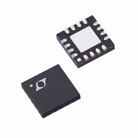
LTC5100EUF#PBF Linear Technology, LTC5100EUF#PBF Datasheet - Page 30

LTC5100EUF#PBF
Manufacturer Part Number
LTC5100EUF#PBF
Description
IC DRIVER VCSEL 3.2GBPS 16QFN
Manufacturer
Linear Technology
Type
Laser Diode Driverr
Datasheet
1.LTC5100EUF.pdf
(52 pages)
Specifications of LTC5100EUF#PBF
Data Rate
3.2Gbps
Number Of Channels
1
Voltage - Supply
3.135 V ~ 3.465 V
Current - Supply
54mA
Current - Modulation
12mA
Operating Temperature
-40°C ~ 85°C
Package / Case
16-QFN
Mounting Type
Surface Mount
Lead Free Status / RoHS Status
Lead free / RoHS Compliant
Available stocks
Company
Part Number
Manufacturer
Quantity
Price
OPERATIO
LTC5100
Conversion Sequence
The ADC has a 1ms conversion time and operates in a four-
cycle sequence. Three of these cycles are dedicated to the
needs of the servo controllers for laser bias and modula-
tion current. One cycle is available to the user to convert
any desired quantity. Table 2 shows how the four conver-
sion time slots are allocated. The temperature compensa-
tion and servo loop calculations are done during the User
cycle. The source and modulation DACs are also updated
during this cycle.
Table 2. ADC Conversion Sequence
CYCLE
1
2
3
4
User Access to the ADC
The results of each conversion cycle in Table 2 are stored
in user accessible registers. The last die temperature
measurement can be read over the I
reading the T_INT_ADC register. Note that the quantity
converted during the third cycle depends on whether the
chip is in APC or CCC mode. The result of the third
conversion cycle is stored in a register that is called
IMD_ADC in APC mode and IS_ADC in CCC mode. There
is only one register, but it is given two names to indicate
the quantity it actually holds.
The fourth cycle, called the user cycle, is available to
digitize any of the six multiplexed signals. The result can
be read out over the I
digitized during the user cycle is selected by setting the
three-bit field USER_ADC.Adc_src_sel (see Table 23).
For example, setting Adc_ src_sel = 2 programs the
multiplexer to select the laser diode voltage, V
the next user conversion cycle, V
stored to the USER_ADC. Data field. When the conversion
is
USER_ADC.Adc_src indicates the signal source whose
converted value is stored in USER_ADC.Data. Reading or
30
complete,
APC MODE
T
I
I
User
M
MD
U
USER_ADC.Valid
2
C serial bus. The signal to be
CCC MODE
T
I
I
User
M
S
2
LD
C bus at any time by
is converted and
RESULT STORED IN
REGISTER
T_INT_ADC
IM_ ADC
IMD_ADC/IS_ADC
USER_ADC
is
LD
set
. During
and
writing the USER_ADC register clears the Valid bit. The
Valid bit remains cleared until the next user conversion is
complete. USER_ADC.Adc_src always corresponds to
the signal source whose data is stored in USER_ADC.Data,
not the source that was most recently selected by writing
USER_ADC.Adc_src_sel. The Valid bit and ADC_src field
are useful for monitoring when the ADC has updated the
USER_ADC.Data field. Table 3 gives an extended example
of accessing the USER_ADC register.
Note that the content of the USER_ADC register is different
for writing and for reading, even though the I
used to access this register is the same in both cases. See
Table 23 and Table 24 for a detailed definition of the bit
fields in the USER_ADC register. Table 23 also shows how
to convert ADC digital codes to real-world quantities.
DIRECT MICROPROCESSOR CONTROL OF THE LASER
BIAS AND MODULATION CURRENT
Setting Lpc_en to zero turns off the LTC5100’s digital
Laser Power Controller (see Figure 2). The source and
modulation DACs (Is_dac and Im_dac) can then be written
from the I
sor or test computer to directly control the source and
modulation currents.
DIGITAL CONTROL AND THE I
The LTC5100 has extensive digital control and monitoring
features. These features can be used during final assembly
of a transceiver module to set up the laser and verify
performance. In normal operation, the LTC5100 can oper-
ate standalone or under microprocessor supervision. Op-
erating standalone, the LTC5100 automatically loads its
configuration and laser operating parameters (bias cur-
rent, modulation current, monitor diode current) from a
small external EEPROM at power up. Operating under
microprocessor supervision, the microprocessor is in
total control of setting up the LTC5100.
I
The digital interface for the LTC5100 is I
bus standard that is fully documented in “I
2
C Serial Interface Protocol
2
C serial bus, allowing an external microproces-
2
C SERIAL INTERFACE
2
C, a 2-wire serial
2
C-Bus and How
2
C command
sn5100 5100fs


