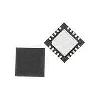
SI3500-A-GM Silicon Laboratories Inc, SI3500-A-GM Datasheet - Page 9

SI3500-A-GM
Manufacturer Part Number
SI3500-A-GM
Description
IC POE SWITCH PWR OVER LAN 20QFN
Manufacturer
Silicon Laboratories Inc
Type
Power over Ethernet Switch (PoE)r
Datasheet
1.SI3500-A-GM.pdf
(18 pages)
Specifications of SI3500-A-GM
Package / Case
20-QFN
Applications
IP Phones, Power over LAN, Network Routers and Switches
Internal Switch(s)
Yes
Current Limit
525mA
Voltage - Supply
42 V ~ 57 V
Operating Temperature
-40°C ~ 85°C
Mounting Type
Surface Mount
Minimum Operating Temperature
- 10 C
Mounting Style
SMD/SMT
Product
Ethernet Controllers
Maximum Operating Temperature
+ 85 C
Lead Free Status / RoHS Status
Lead free / RoHS Compliant
Lead Free Status / RoHS Status
Lead free / RoHS Compliant, Lead free / RoHS Compliant
Other names
336-1844-5
Available stocks
Company
Part Number
Manufacturer
Quantity
Price
Company:
Part Number:
SI3500-A-GM
Manufacturer:
MURATA
Quantity:
34 000
Part Number:
SI3500-A-GM
Manufacturer:
SILICON LABS/芯科
Quantity:
20 000
Part Number:
SI3500-A-GMR
Manufacturer:
SILICON LABS/芯科
Quantity:
20 000
3. Functional Description
3.1. Input Surge Protection
The Si3500 has a 65 V Zener diode clamp on the input
between VPOS1 and VNEG. The diode is designed to
limit the input voltage to less than 80 V for surges of up
to 5 A and 50 µsec duration. This provides protection
against hot plugging the input power supply.
If the input power supply is hot plugged and there is no
surge limiting resistance, there can be an overshoot of
input voltage due to lead inductance. For this reason, an
optional surge limiting resistor of 2 is recommended.
This is particularly true if EMC reduction capacitor is
placed directly across VPOS and VNEG.
3.2. Under Voltage Lockout
The Si3500 incorporates an undervoltage lockout
(UVLO) circuit to monitor the line voltage and determine
when to activate the integrated switching regulator.
Before power is applied to the switching regulator, the
hotswap switch output (HSO) pin is high-impedance
and typically follows VPOS as the input is ramped (due
to the discharged switcher supply capacitor). When the
input voltage rises above the UVLO turn-on threshold
(42 V maximum), the Si3500 turns on the internal
hotswap power MOSFET. The switcher supply capacitor
begins to charge up under the current limit control of the
Si3500, and the HSO pin transitions from VPOS to
VNEG. The Si3500 includes hysteresis in UVLO circuits
to maintain power to the load until the input voltage falls
below the UVLO turn-off threshold. Once the input
voltage falls below 30 V (minimum), the internal
hotswap MOSFET is turned off.
3.3. Dual Current Limit Hot Swap switch
The Si3500 implements dual current limits. While the
hotswap MOSFET is charging the switcher supply
capacitor, the Si3500 maintains a lower current limit.
The switching regulator is disabled until the voltage
across the hotswap MOSFET becomes sufficiently low,
indicating the switcher supply capacitor is almost
completely charged. When this threshold is reached,
the switcher is activated, and the hotswap current limit
is increased. This threshold also has hysteresis to
prevent systemic oscillation as the switcher begins to
draw current and the current limit is increased.
The Si3500 stays in a high-level current limit mode until
the input voltage drops below the UVLO turn-off
threshold or excessive power is dissipated in the
hotswap switch. This dual-level current limit gives low
current draw from the input power supply during normal
start up with the higher current only occurring during
fault conditions.
Rev. 1.1
3.4. Switching Regulator
The Si3500 can be configured to provide output that is
either more positive, more negative, or isolated from the
positive terminal of the input power supply.
The application determines the converter topology. An
isolated application will require a flyback transformer-
based
application can use an inductor-based buck converter
topology. In the isolated case, dc isolation is achieved
through a transformer in the forward path and a voltage
reference plus opto-isolator in the feedback path. The
application circuit shown in Figure 2 is an example of
such a topology. The non-isolated application in
Figure 1 makes use of a single inductor as the energy
conversion element, and the feedback signal is directly
supplied into the internal error amplifier. The approach
shown in Figure 3 is for a non-isolated application
where the output is more positive than the input.
3.5. Switcher Startup
The switching regulator is disabled until the hotswap
interface has charged the supply capacitor needed to
filter the switching regulator's high-current transients.
Once the supply capacitor is charged, the hotswap
controller engages the internal bias currents and
supplies used by the switcher. Additionally, the soft-start
current begins to charge the external soft-start
capacitor.
The voltage developed across the soft-start capacitor
serves as the error amplifier's reference in the non-
isolated application. Ramping this voltage slowly allows
the switching regulator to bring up the regulated output
voltage in a controlled manner. Controlling the initial
startup of the regulated voltage restrains power
dissipation in the switching FET and prevents overshoot
and ringing in the output supply voltage.
In the isolated mode, a capacitor connected between
pins ISOSSFT and VSSA slowly ramps the duty cycle
clamp in the PWM circuit. Tie the ISOSSFT pin to VDD
if not used.
3.6. Switching Regulator Operation
The switching regulator of the Si3500 is a constant-
frequency, pulse-width-modulated (PWM) controller
integrated with switching power FET optimized for the
output power range of up to 10 W.
Once the hotswap interface has ensured proper turn-on
of the switching regulator controller, the switcher is fully
operational. An internal free-running oscillator and
internal precision voltage reference are fed into the
pulse-width modulator. The output of the error amplifier
(either internal for non-isolated applications or external
switching
topology
while
a
Si3500
non-isolated
9


