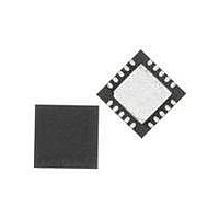
SI3500-A-GM Silicon Laboratories Inc, SI3500-A-GM Datasheet - Page 10

SI3500-A-GM
Manufacturer Part Number
SI3500-A-GM
Description
IC POE SWITCH PWR OVER LAN 20QFN
Manufacturer
Silicon Laboratories Inc
Type
Power over Ethernet Switch (PoE)r
Datasheet
1.SI3500-A-GM.pdf
(18 pages)
Specifications of SI3500-A-GM
Package / Case
20-QFN
Applications
IP Phones, Power over LAN, Network Routers and Switches
Internal Switch(s)
Yes
Current Limit
525mA
Voltage - Supply
42 V ~ 57 V
Operating Temperature
-40°C ~ 85°C
Mounting Type
Surface Mount
Minimum Operating Temperature
- 10 C
Mounting Style
SMD/SMT
Product
Ethernet Controllers
Maximum Operating Temperature
+ 85 C
Lead Free Status / RoHS Status
Lead free / RoHS Compliant
Lead Free Status / RoHS Status
Lead free / RoHS Compliant, Lead free / RoHS Compliant
Other names
336-1844-5
Available stocks
Company
Part Number
Manufacturer
Quantity
Price
Company:
Part Number:
SI3500-A-GM
Manufacturer:
MURATA
Quantity:
34 000
Part Number:
SI3500-A-GM
Manufacturer:
SILICON LABS/芯科
Quantity:
20 000
Part Number:
SI3500-A-GMR
Manufacturer:
SILICON LABS/芯科
Quantity:
20 000
Si3500
for isolated applications) is also routed into the PWM
and determines the slicing of the oscillator.
The PWM controls the switching FET drive circuitry. A
significant advantage of integrating the switching power
FET onto the same monolithic IC as the switching
regulator controller is the ability to precisely adjust the
drive strength and timing to the FET's sizable gate,
resulting in high regulator efficiency. Furthermore,
current-limiting circuitry prevents the switching FET
from sinking too much current, dissipating too much
power, and becoming damaged. Thermal overload
protection provides a secondary level of protection.
The flexibility of the Si3500's switching regulator allows
the system designer to realize either the isolated or non-
isolated application circuitry using a single device. In
operation, the integration of the switching FET allows
tighter control and more efficient operation than a
general-purpose switching regulator coupled with a
general-purpose external FET.
10
Rev. 1.1
4. Layout Guidelines
The following are general PCB layout considerations;
reference designs are also available. Due to the unique
high-voltage and high-power design considerations,
Silicon Labs recommends that the reference designs be
followed closely for both BOM and layout. Visit the
Silicon Labs Technical Support web page and register to
submit a technical support request, particularly if you
are not closely following the recommended reference
design.
Care must be taken to connect the thermal pad of the
Si3500 to an appropriate heat spreader. For full-power
applications, a 2 square in plane with at least 9 thermal
vias is recommended. This heat spreader must be
electrically connected to the negative input power
supply.
Care must also be taken in layout to avoid EMI and
EMC. Input and output filter capacitors are normally
ceramic capacitors for high-frequency performance in
parallel with electrolytic capacitors for load transient
performance. The ceramic capacitors in particular
should be placed so as to minimize radiation for the
high-current paths of the switching regulator. The
circular area of current flow with the FET on and FET off
should be minimized. The direction of current flow with
FET on and FET off should maintain a constant
clockwise or counterclockwise rotation.
For EMI reduction, a 4 layer design with inner layers
connected to the positive input and Vss (for isolated
applications) or Vout (for non-isolated applications) is
recommended. The high-current paths should not flow
through these shield planes. Connection of the dc-to-dc
converter high-current paths to the shield plane should
be at a single point. Refer to the Si3452 reference
design databases for additional layout guideline details.


