SI3500-A-GM Silicon Laboratories Inc, SI3500-A-GM Datasheet
SI3500-A-GM
Specifications of SI3500-A-GM
Available stocks


Related parts for SI3500-A-GM

SI3500-A-GM Summary of contents
Page 1
... The Si3500 can be configured to provide an isolated output voltage or a non-isolated output that is positive or negative with respect to the positive input rail. Input undervoltage and overvoltage lockout functions are fully-integrated. ...
Page 2
... Si3500 Functional Block Diagram Central Protection Bias VNEG 2 Error Amplifier PWM Soft Start Control Si3500 Rev. 1.1 SWO ...
Page 3
... Dual Current Limit Hot Swap switch . . . . . . . . . . . . . . . . . . . . . . . . . . . . . . . . . . . . . .9 3.4. Switching Regulator . . . . . . . . . . . . . . . . . . . . . . . . . . . . . . . . . . . . . . . . . . . . . . . . . .9 3.5. Switcher Startup . . . . . . . . . . . . . . . . . . . . . . . . . . . . . . . . . . . . . . . . . . . . . . . . . . . . .9 3.6. Switching Regulator Operation . . . . . . . . . . . . . . . . . . . . . . . . . . . . . . . . . . . . . . . . . .9 4. Layout Guidelines . . . . . . . . . . . . . . . . . . . . . . . . . . . . . . . . . . . . . . . . . . . . . . . . . . . . . . . 10 5. Pin Descriptions . . . . . . . . . . . . . . . . . . . . . . . . . . . . . . . . . . . . . . . . . . . . . . . . . . . . . . . . . 11 6. Package Outline . . . . . . . . . . . . . . . . . . . . . . . . . . . . . . . . . . . . . . . . . . . . . . . . . . . . . . . . . 13 7. Recommended PCB Landing Pattern . . . . . . . . . . . . . . . . . . . . . . . . . . . . . . . . . . . . . . . . 14 8. Ordering Guide . . . . . . . . . . . . . . . . . . . . . . . . . . . . . . . . . . . . . . . . . . . . . . . . . . . . . . . . . . 16 Document Change List . . . . . . . . . . . . . . . . . . . . . . . . . . . . . . . . . . . . . . . . . . . . . . . . . . . . .17 Contact Information . . . . . . . . . . . . . . . . . . . . . . . . . . . . . . . . . . . . . . . . . . . . . . . . . . . . . . . .18 Rev. 1.1 Si3500 Page 3 ...
Page 4
... Si3500 1. Electrical Specifications Table 1. Recommended Operating Conditions Description VPOS – VNEG input voltage Ambient Operating Temperature Note: Unless otherwise noted, all voltages referenced to VNEG. All minimum and maximum specifications are guaranteed and apply across the recommended operating conditions. Typical values apply at nominal supply voltage and ambient temperature unless otherwise noted ...
Page 5
... Permanent device damage may occur if the maximum ratings are exceeded. Functional operation should be restricted to those conditions specified in the operational sections of this data sheet. Exposure to absolute maximum rating conditions for extended periods may adversely affect device reliability. 2. Care should be taken to follow layout guidelines. 1 Description 1,2 Description Rev. 1.1 Si3500 Rating Unit –0 –0 –0 – ...
Page 6
... Si3500 Table 5. Electrical Characteristics Parameter 1 Current Limit Hotswap FET On-Resistance + R SENSE Switcher Frequency Maximum Switcher Duty Cycle Switching FET On-Resistance 2 Regulated Feedback @ pin FB Regulated Output Voltage Tolerance VDD accuracy @ 0.8 mA Softstart charging current Thermal Shutdown Thermal Shutdown Hysteresis Notes turn-on, before the HSO load capacitor is charged, the current limit is set at the inrush level. After the capacitor has been charged within ~1 ...
Page 7
... RBIAS C1 Figure 2. Schematic (Isolated 3.3 V Output)* *Note: This is a simplified schematic. Refer to Si3452 reference design databases for complete application schematic. Cssft FB RBIAS Si3500 SWO VNEG EROUT SWO C8 ISOSSFT PS2911 VDD Si3500 R2 EROUT Rev. 1.1 Si3500 +VOUT 3.3 V Cout 68µH -VOUT Ccomp ...
Page 8
... RBIAS to reduce Short circuit current limit C1 EROUT Figure 3. Schematic—Non-Isolated 3.3 V Output* *Note: This is a simplified schematic. Refer to Si3452 reference design databases for complete application schematic. Figure 4. Startup Waveform for Current in Figure SWO C8 ISOSSFT PS2911 VDD Si3500 R2 EROUT Rev. 1 Connect to +Vin ...
Page 9
... Functional Description 3.1. Input Surge Protection The Si3500 has Zener diode clamp on the input between VPOS1 and VNEG. The diode is designed to limit the input voltage to less than 80 V for surges and 50 µsec duration. This provides protection against hot plugging the input power supply. ...
Page 10
... Care must be taken to connect the thermal pad of the Si3500 to an appropriate heat spreader. For full-power applications square in plane with at least 9 thermal vias is recommended. This heat spreader must be electrically connected to the negative input power supply ...
Page 11
... Pin Descriptions ISOSSFT Table 8. Si3500 Pin Descriptions (Top View) Pin# Name 1 EROUT Error-amplifier output and PWM input; directly connected to opto-coupler in isolated or boost applications. 2 SSFT Soft-start output pin ramps voltage across external soft-start capacitor to allow switcher to ramp output slowly. 3 VDD 5 V supply rail for switcher; provides drive for opto-coupler. ...
Page 12
... Si3500 Table 8. Si3500 Pin Descriptions (Top View) (Continued) 16 VPOS2 High-voltage supply, positive rail sense node. 17 VSS1 Negative supply rail for switcher; externally tied to HSO. 18 SWO Switching transistor output; drain of switching N-FET. 19 VSS2 Negative supply rail for switcher; externally tied to HSO Regulated feedback input in non-isolated application. ...
Page 13
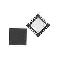
... Package Outline Figure 5 illustrates the package details for the Si3500. Table 9 lists the values for the dimensions shown in the illustration. Figure 5. 20-Lead Quad Flat No-Lead Package (QFN) Dimension aaa bbb ccc ddd Notes: 1. All dimensions shown are in millimeters (mm) unless otherwise noted. ...
Page 14
... Si3500 7. Recommended PCB Landing Pattern 14 Figure 6. PCB Land Pattern Rev. 1.1 ...
Page 15
... A 2x2 array of 1.2 mm square openings on 1.4 mm pitch should be used for the center ground pad. Card Assembly No-Clean, Type-3 solder paste is recommended. 10. The recommended card reflow profile is per the JEDEC/IPC J-STD-020C specification for Small Body Components. Nom Max 2.75 2.80 2.75 2.80 0.30 0.35 0.95 1.00 4.70 4.70 0.80 Rev. 1.1 Si3500 15 ...
Page 16
... Si3500 8. Ordering Guide * Part Number Si3500-A-GM 20-pin QFN, RoHS compliant *Note: Add an “R” at the end of the part number to denote tape and reel option. 16 Package Temp Range – °C Rev. 1.1 Recommended Maximum Output Power < ...
Page 17
... OCUMENT HANGE IST Revision 0.1 to Revision 1.0 Updated revision number to 1.0 to reflect production status. Updated Table 4 on page 5. Revision 1.0 to Revision 1.1 Editorial changes in "4. Layout Guidelines" on page 10. Rev. 1.1 Si3500 17 ...
Page 18
... Si3500 C I ONTACT NFORMATION Silicon Laboratories Inc. 400 West Cesar Chavez Austin, TX 78701 Tel: 1+(512) 416-8500 Fax: 1+(512) 416-9669 Toll Free: 1+(877) 444-3032 Please visit the Silicon Labs Technical Support web page: https://www.silabs.com/support/pages/contacttechnicalsupport.aspx and register to submit a technical support request. The information in this document is believed to be accurate in all respects at the time of publication but is subject to change without notice. ...