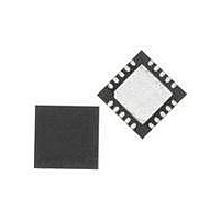
SI3500-A-GM Silicon Laboratories Inc, SI3500-A-GM Datasheet - Page 15

SI3500-A-GM
Manufacturer Part Number
SI3500-A-GM
Description
IC POE SWITCH PWR OVER LAN 20QFN
Manufacturer
Silicon Laboratories Inc
Type
Power over Ethernet Switch (PoE)r
Datasheet
1.SI3500-A-GM.pdf
(18 pages)
Specifications of SI3500-A-GM
Package / Case
20-QFN
Applications
IP Phones, Power over LAN, Network Routers and Switches
Internal Switch(s)
Yes
Current Limit
525mA
Voltage - Supply
42 V ~ 57 V
Operating Temperature
-40°C ~ 85°C
Mounting Type
Surface Mount
Minimum Operating Temperature
- 10 C
Mounting Style
SMD/SMT
Product
Ethernet Controllers
Maximum Operating Temperature
+ 85 C
Lead Free Status / RoHS Status
Lead free / RoHS Compliant
Lead Free Status / RoHS Status
Lead free / RoHS Compliant, Lead free / RoHS Compliant
Other names
336-1844-5
Available stocks
Company
Part Number
Manufacturer
Quantity
Price
Company:
Part Number:
SI3500-A-GM
Manufacturer:
MURATA
Quantity:
34 000
Part Number:
SI3500-A-GM
Manufacturer:
SILICON LABS/芯科
Quantity:
20 000
Part Number:
SI3500-A-GMR
Manufacturer:
SILICON LABS/芯科
Quantity:
20 000
General:
Solder Mask Design:
Stencil Design:
Card Assembly:
1. All dimensions shown are in millimeters (mm) unless otherwise noted.
2. Dimensioning and Tolerancing is per the ANSI Y14.5M-1994 specification.
3. This Land Pattern Design is based on the IPC-7351 guidelines.
4. All metal pads are to be non-solder mask defined (NSMD). Clearance between the
5. A stainless steel, laser-cut and electro-polished stencil with trapezoidal walls should be
6. The stencil thickness should be 0.125mm (5 mils).
7. The ratio of stencil aperture to land pad size should be 1:1 for all perimeter pins.
8. A 2x2 array of 1.2 mm square openings on 1.4 mm pitch should be used for the center
9. A No-Clean, Type-3 solder paste is recommended.
10. The recommended card reflow profile is per the JEDEC/IPC J-STD-020C specification
Symbol
solder mask and the metal pad is to be 60 m minimum, all the way around the pad.
used to assure good solder paste release.
ground pad.
for Small Body Components.
P1
P2
X1
Y1
C1
C2
E
Table 10. PCB Land Pattern Dimensions
2.70
2.70
0.25
0.90
Min
Rev. 1.1
Nom
2.75
2.75
0.30
0.95
4.70
4.70
0.80
Max
2.80
2.80
0.35
1.00
Si3500
15


