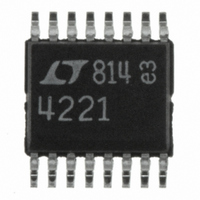
LTC4221CGN#PBF Linear Technology, LTC4221CGN#PBF Datasheet - Page 22

LTC4221CGN#PBF
Manufacturer Part Number
LTC4221CGN#PBF
Description
IC CTLR HOT SWAP DUAL 16SSOP
Manufacturer
Linear Technology
Type
Hot-Swap Controllerr
Datasheet
1.LTC4221CGNPBF.pdf
(28 pages)
Specifications of LTC4221CGN#PBF
Applications
General Purpose
Internal Switch(s)
No
Voltage - Supply
1 V ~ 13.5 V
Operating Temperature
0°C ~ 70°C
Mounting Type
Surface Mount
Package / Case
16-SSOP (0.150", 3.90mm Width)
Lead Free Status / RoHS Status
Lead free / RoHS Compliant
Available stocks
Company
Part Number
Manufacturer
Quantity
Price
APPLICATIO S I FOR ATIO
LTC4221
supply voltages, the LTC4221 can drive any MOSFET rated
with 4.5V or 2.5V gate drive. For higher supply voltages up
to 13.5V, the LTC4221 can drive any MOSFET rated with
a 10V or 4.5V gate drive. The selected MOSFET should
fulfill two V
1. Positive V
2. Negative V
If one of the conditions cannot be met, an external zener
clamp shown on Figure 15 can be used. The clamp
network is connected from each channel’s GATE to the
V
the current flow into the GATE n pin’s internal zener clamp
during transient events.
A MOSFET with a V
meets the two criteria for all the LTC4221 application ranges
from 1V to 13.5V. Typically most 10V gate rated MOSFETs
have V
no external V
rated MOSFETs with V
±20V. In addition to the MOSFET gate drive rating and V
absolute maximum rating, other criteria such as V
I
operating area (SOA) should also be carefully reviewed.
V
sive of spikes and ringing. I
mum short-circuit current in the channel during a fault
22
D(MAX)
OUT
BDSS
maximum ΔV
age. The gate of the MOSFET can discharge faster than
V
C
OUT
LOAD
pins. V
GS
should exceed the maximum supply voltage inclu-
, R
when shutting down the MOSFET with a large
.
absolute maximum ratings of ±20V or greater, so
*USER SELECTED VOLTAGE CLAMP
(A LOW BIAS CURRENT ZENER DIODE IS RECOMMENDED)
1N4688 (5V)
1N4692 (7V): LOGIC-LEVEL MOSFET
1N4695 (9V)
1N4702 (15V): STANDARD-LEVEL MOSFET
DS(ON)
Figure 15. Gate Protection Zener Clamp
GS
GS
GS
GS
GS
V
criteria:
CC
is clamped in both directions and R
zener clamp is needed. There are 4.5V gate
absolute maximum rating > LTC4221’s
GATE
absolute maximum rating > supply volt-
, P
R
SENSE
GS
U
D
.
, θ
absolute maximum rating of ±20V
GS
GATE
Q1
JA
U
R
200Ω
absolute maximum ratings of
, T
G
D(MAX)
D1*
J(MAX)
D2*
must exceed the maxi-
W
and maximum safe
4221 F15
V
OUT
U
G
limits
BDSS
GS
,
condition. R
gether with V
example, at 1V V
V
be relaxed in which case the MOSFET’s thermal require-
ments (P
The power dissipated in the MOSFET is (I
and this should be less than the maximum power dissipa-
tion, P
the MOSFET junction temperature, T
from the operating temperature (T
package thermal resistance (θ
be less than the T
figure must also be well within the manufacturer’s recom-
mended safe operating area (SOA) with sufficient margin.
These three thermal parameters must not be exceeded for
all conditions in a channel including normal mode opera-
tion, start-up with or without current limit, fault and
autoretry after a fault. To ensure a reliable design, fault
tests should be evaluated in the laboratory.
V
Good engineering practice calls for bypassing the supply
rail of any analog circuit. Bypass capacitors are often
placed at the supply connection of every active device, in
addition to one or more large value bulk bypass capacitors
per supply rail. If power is connected abruptly, the large
bypass capacitors slow the rate of rise of the supply
voltage and heavily damp any parasitic resonance of lead
or PC track inductance working against the supply bypass
capacitors.
The opposite is true for LTC4221 Hot Swap circuits
mounted on plug-in cards since controlling the surge
current to bypass capacitors at plug-in is the primary
motivation for the Hot Swap controller. In most cases,
there is no supply bypass capacitor present on the pow-
ered supply voltage side of the MOSFET switch. Although
wire harness, backplane and PCB trace inductances are
usually small, these can create large spikes when large
currents are suddenly drawn, cut off or limited. Abrupt
intervention can prevent subsequent damage caused by a
catastrophic fault but it does cause a large supply tran-
sient. These ringing transients appear as a fast edge on
OUT2
CC
Transient Protection
error. At higher V
D
, allowed in that package. Given power dissipation,
D
, T
DS(ON)
RSENSE
J(MAX)
CC2
determines the MOSFET V
J(MAX)
, SOA) may limit the value of R
yields an error in the V
, V
CC
DS
voltages the V
+ V
specification. The V
RSENSE2
JA
). The operating T
A
) and the MOSFET
= 50mV gives a 5%
J
DS
can be computed
LOAD
requirement can
OUT
DS
)
voltage. For
2
DS
which to-
• R
J
• I
DS(ON)
should
DS(ON)
LOAD
4221fa
.


