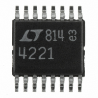
LTC4221CGN#PBF Linear Technology, LTC4221CGN#PBF Datasheet - Page 20

LTC4221CGN#PBF
Manufacturer Part Number
LTC4221CGN#PBF
Description
IC CTLR HOT SWAP DUAL 16SSOP
Manufacturer
Linear Technology
Type
Hot-Swap Controllerr
Datasheet
1.LTC4221CGNPBF.pdf
(28 pages)
Specifications of LTC4221CGN#PBF
Applications
General Purpose
Internal Switch(s)
No
Voltage - Supply
1 V ~ 13.5 V
Operating Temperature
0°C ~ 70°C
Mounting Type
Surface Mount
Package / Case
16-SSOP (0.150", 3.90mm Width)
Lead Free Status / RoHS Status
Lead free / RoHS Compliant
Available stocks
Company
Part Number
Manufacturer
Quantity
Price
APPLICATIO S I FOR ATIO
LTC4221
Timer Function
The TIMER pin controls the initial cycle and the channel
start-up cycles with an external capacitor, C
are two comparator thresholds: V
V
current, a 20μA pull-up current and a N-channel MOSFET
pull-down.
Initial Timing Cycle
When the card is being inserted into the bus connector, the
long pins mate first which brings up the supplies at time
point 1 of Figure 13. The LTC4221 is in reset mode as the
ON1 pin is low. Both GATE pins and the TIMER pin are
pulled low. At time point 2, the short pin makes contact and
both ON pins are pulled high. At this instant, a start-up
check requires that both supply voltages be above UVLO,
at least one ON pin be above 0.851V, both GATE pins
< 0.4V and TIMER < 0.4V. When these four conditions are
fulfilled, the initial cycle begins and the TIMER pin is pulled
high with 1.9μA. At time point 3, the TIMER reaches
V
channel MOSFET pull-down, ending the initial cycle at time
point 4. The initial cycle delay is:
20
TMR(L)
TMR(H)
t
TIMER
GATE1
INITIAL
V
V
OUT1
ON n
CC n
Figure 13. Channel 1 Start-Up Without Current Limit
(0.4V). In addition, the pin has a 1.9μA pull-up
and is pulled down below V
RESET
STATE
=
0.851V
1 234
.
1 2
1.9μA
1.234V
INITIAL
TIMING
V
U
•
3 4 5
C
1 9
TIMER
.
CHANNEL 1
START-UP
U
0.4V
9.5μA
20μA
μ
V
A
TH
6
NORMAL
W
TMR(H)
0.4V
TMR(L)
7
(1.234V) and
TIMER
4221 F13
DISCHARGE
BY LOAD
U
by the N-
. There
(9)
At time point 4, the LTC4221 checks whether the FILTER
pin is <1.24V and FAULT is > 0.851V. If both conditions are
met, a channel start-up cycle commences.
Start-Up Cycle Without Current Limit
During a channel start-up cycle, the TIMER pin ramps up
with a 20μA internal pull-up so the start-up cycle delay is:
At the beginning of the start-up timing cycle (time point 4),
the LTC4221’s electronic circuit breaker is armed and each
channel has an internal 9.5μA current source working with
an internal charge pump to provide the gate drive to its
external pass transistor. At time point 5, GATE1 reaches
the external pass transistor threshold and V
follow the GATE1 ramp-up. If the inrush current is below
current limit, GATE1 ramps at a constant rate of:
where C
inrush current through R
components; I
C
The load bypass capacitance typically dominates C
For a successful channel start-up without current limit,
I
configuration, the V
V
current limit is :
At time point 6, V
ramp-up continues until it reaches a maximum voltage.
This maximum voltage is determined either by the charge
pump or the internal clamp.
INRUSH
LOAD
GATE1
I
I
I
t
Δ
INRUSH
INRUSH
INRUSH
STARTUP
V
Δ
GATE
and I
. The inrush current during a start-up cycle without
T
GATE
< active current limit. Due to the voltage follower
=
=
=
LOAD
=
is the total capacitance at the GATE1 pin. The
=
⎛
⎜
⎝
⎛
⎜
⎝
⎛
⎜
⎝
C
I
C
C
C
(
CLOAD
GATE
GATE
LOAD
LOAD
LOAD
1 234
due to the noncapacitive load elements.
.
OUT1
OUT1
•
•
•
due to the total load capacitance
V
C
Δ
Δ
is approximately V
I
GATE
– .
GATE
V
V
Δ
ramp rate approximately tracks
SENSE1
Δ
GATE
0 4
OUT
T
T
V
⎞
⎟ +
⎠
⎞
⎟ +
⎠
)
⎞
⎟ +
⎠
•
can be divided into two
I
LOAD
I
C
LOAD
20
I
LOAD
TIMER
μ
A
CC1
OUT1
but GATE1
starts to
LOAD
(10)
(11)
(12)
4221fa
.


