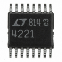
LTC4221CGN#PBF Linear Technology, LTC4221CGN#PBF Datasheet - Page 14

LTC4221CGN#PBF
Manufacturer Part Number
LTC4221CGN#PBF
Description
IC CTLR HOT SWAP DUAL 16SSOP
Manufacturer
Linear Technology
Type
Hot-Swap Controllerr
Datasheet
1.LTC4221CGNPBF.pdf
(28 pages)
Specifications of LTC4221CGN#PBF
Applications
General Purpose
Internal Switch(s)
No
Voltage - Supply
1 V ~ 13.5 V
Operating Temperature
0°C ~ 70°C
Mounting Type
Surface Mount
Package / Case
16-SSOP (0.150", 3.90mm Width)
Lead Free Status / RoHS Status
Lead free / RoHS Compliant
Available stocks
Company
Part Number
Manufacturer
Quantity
Price
APPLICATIO S I FOR ATIO
LTC4221
sequential power up from time points 4 to 8 and a
sequential power-down programmed from time points 9
to 11. To achieve this the circuit requires the functionality
of the PWRGD1 pin and will be featured in the next section.
The circuit in Figure 2a sits on a daughter board with
staggered pins on its edge connectors. Supply voltage and
ground connections are wired to long-edge connector
pins while both ON pins are connected to a short-edge
connector pin through a resistive divider. Until the con-
nectors are fully mated, ON1 is pulled low and holds both
channels in the reset state. When the connectors have
properly seated, the ON pins are pulled above 0.851V and
an initial timing cycle starts. This cycle is restarted by any
transitions on the ON pins across their off thresholds and
adds a further delay for the plug-in transients to die off
before allowing a start-up cycle. The Typical Application
circuit on the first page of this data sheet shows similar
14
U
PWRGD1
TIMER
GATE1
GATE2
V
V
V
OUT1
OUT2
ON1
ON2
CC n
U
V
CC n (UVL)
UVLO
0.851V
W
RESET
Figure 3. Sequential Power On/Off Timing Waveforms
1 2
1.9μA
1.234V
INITIAL
TIMING
3 4
CHANNEL 1
START-UP
U
9.5μA
20μA
V
TH
5 6 7
V
FB1
CHANNEL 2
= 0.620V
START-UP
20μA
0.851V
9.5μA
V
TH
considerations in the design of its PCB edge connectors,
and the resistive dividers connected to ON1 and ON2 act
as an external UVLO to override the internal one. An RC
filter can be added at the ON1 pin to increase the delay time
at card insertion to allow bus supply transients to stabilize.
FB and PWRGD Pin Functions
Each FB pin is used to detect undervoltage and overvoltage
in its channel output voltage (V
divider. Each FB pin has an undervoltage comparator with
a high-to-low threshold of 0.617V and 3mV hysteresis.
The output of this comparator controls the channel’s
open-drain PWRGD output. During UVLO, both PWRGD
pins are pulled low by internal N-channel MOSFET pull-
downs. As both channels come out of UVLO, control of
PWRGD1 is passed to FB1and control of PWRGD2 to FB2.
Each PWRGD pin can be connected to a pull-up resistor to
8
NORMAL
V
FB1
0.821V
CHANNEL 2 NORMAL
= 0.617V
0.4V
CHANNEL 1 OFF
9 10 11
100μA
OFF
0.821V
100μA
DISCHARGE
BY LOAD
DISCHARGE
BY LOAD
4221 F03
OUT
) through a resistive
4221fa


