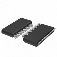
PCF85162T/1,118 NXP Semiconductors, PCF85162T/1,118 Datasheet - Page 27

PCF85162T/1,118
Manufacturer Part Number
PCF85162T/1,118
Description
IC LCD DISPLAY DVR 32SEG 48TSSOP
Manufacturer
NXP Semiconductors
Datasheet
1.PCF85162T1118.pdf
(43 pages)
Specifications of PCF85162T/1,118
Package / Case
48-TSSOP
Display Type
LCD
Configuration
32 Segment
Interface
I²C
Digits Or Characters
Any Digit Type
Current - Supply
8µA
Voltage - Supply
1.8 V ~ 5.5 V
Operating Temperature
-40°C ~ 85°C
Mounting Type
Surface Mount
Number Of Digits
16
Number Of Segments
128
Maximum Clock Frequency
400 KHz
Operating Supply Voltage
1.8 V to 5.5 V
Maximum Power Dissipation
400 mW
Maximum Operating Temperature
+ 85 C
Attached Touch Screen
No
Maximum Supply Current
50 mA
Minimum Operating Temperature
- 40 C
Dc
1123
Lead Free Status / RoHS Status
Lead free / RoHS Compliant
Other names
568-5059-2
NXP Semiconductors
10. Static characteristics
Table 16.
V
[1]
[2]
[3]
[4]
[5]
[6]
[7]
PCF85162_2
Product data sheet
Symbol
Supplies
V
V
I
I
Logic
V
V
V
I
I
I
I
C
LCD outputs
ΔV
R
DD
DD(LCD)
OL
OH(CLK)
L
L(OSC)
DD
DD
LCD
P(POR)
IL
IH
I
O
O
= 1.8 V to 5.5 V; V
V
LCD outputs are open-circuit; inputs at V
For typical values, see
For typical values, see
I
also
Periodically sampled, not 100 % tested.
Outputs measured one at a time.
2
LCD
C pins SCL and SDA have no diode to V
Figure
> 3 V for
Static characteristics
Parameter
supply voltage
LCD supply voltage
supply current
LCD supply current
power-on reset supply voltage
LOW-level input voltage
HIGH-level input voltage
LOW-level output current
HIGH-level output current on pin CLK
leakage current
leakage current on pin OSC
input capacitance
output voltage variation
output resistance
18).
1
⁄
3
bias.
SS
Figure 19
Figure 20
= 0 V; V
LCD
= 2.5 V to 6.5 V; T
SS
DD
All information provided in this document is subject to legal disclaimers.
or V
and when tested may therefore be driven to the V
DD
; external clock with 50 % duty factor; I
Rev. 02 — 7 May 2010
Conditions
f
f
on pins CLK, SYNC,
OSC, A0 to A2, SA0,
SCL, SDA
on pins CLK, SYNC,
OSC, A0 to A2, SA0,
SCL, SDA
output sink current;
V
output source current;
V
V
on pins CLK, SCL, SDA,
A0 to A2, and SA0
V
on pins BP0 to BP3 and
S0 to S31
V
clk(ext)
clk(ext)
OL
OH
I
I
LCD
on pins CLK and SYNC
on pin SDA
on pins BP0 to BP3
on pins S0 to S31
amb
= V
= V
= 0.4 V; V
= 4.6 V; V
= 5 V
DD
DD
=
= 1536 Hz
= 1536 Hz
−
or V
40
°
SS
C to +85
DD
DD
;
= 5 V
= 5 V
Universal LCD driver for low multiplex rates
°
C; unless otherwise specified.
[1]
[2][3]
[2][4]
[5]
[6]
[7]
2
C-bus inactive.
I
Min
1.8
2.5
-
-
1.0
V
0.7V
1
3
1
−1
−1
-
−100
-
-
limiting values given in
SS
DD
Typ
-
-
-
-
1.3
-
-
-
-
-
-
-
-
-
1.5
6.0
PCF85162
© NXP B.V. 2010. All rights reserved.
Max
5.5
6.5
20
60
1.6
0.3V
V
-
-
-
+1
+1
7
+100
-
-
DD
Table 15
DD
27 of 43
(see
Unit
V
V
μA
μA
V
V
V
mA
mA
mA
μA
μA
pF
mV
kΩ
kΩ


