PCF85162T/1,118 NXP Semiconductors, PCF85162T/1,118 Datasheet
PCF85162T/1,118
Specifications of PCF85162T/1,118


Related parts for PCF85162T/1,118


PCF85162T/1,118 Summary of contents
Page 1
PCF85162 Universal LCD driver for low multiplex rates Rev. 02 — 7 May 2010 1. General description The PCF85162 is a peripheral device which interfaces to almost any Liquid Crystal Display (LCD) multiplexed LCD containing up to four backplanes and ...
Page 2
... NXP Semiconductors 3. Ordering information Table 1. Type number PCF85162T/1 4. Marking Table 2. Type number PCF85162T/1 5. Block diagram V LCD LCD BIAS GENERATOR V SS CLK CLOCK SELECT AND TIMING SYNC OSC OSCILLATOR V DD SCL INPUT FILTERS SDA Fig 1. Block diagram of PCF85162 PCF85162_2 Product data sheet ...
Page 3
... NXP Semiconductors 6. Pinning information 6.1 Pinning Fig 2. PCF85162_2 Product data sheet S23 1 S24 2 3 S25 4 S26 S27 5 S28 6 S29 7 8 S30 9 S31 SDA 10 SCL 11 SYNC 12 13 CLK OSC SA0 LCD BP0 22 23 BP2 24 BP1 Top view. For mechanical details, see Pinning diagram for PCF85162T All information provided in this document is subject to legal disclaimers. Rev. 02 — ...
Page 4
... NXP Semiconductors 6.2 Pin description Table 3. Symbol SDA SCL SYNC CLK V DD OSC SA0 LCD BP0 to BP3 S0 to S22, S23 to S31 PCF85162_2 Product data sheet Pin description Pin Type 10 input/output 11 input 12 input/output 13 input/output 14 supply 15 input input 19 input 20 supply 21 supply output 26 to 48, ...
Page 5
... NXP Semiconductors 7. Functional description The PCF85162 is a versatile peripheral device designed to interface between any microprocessor or microcontroller to a wide variety of LCD segment or dot matrix displays (see Figure backplanes and segments. Fig 3. The possible display configurations of the PCF85162 depend on the number of active backplane outputs required. A selection of display configurations is shown in of these configurations can be implemented in the typical system shown in Table 4 ...
Page 6
... NXP Semiconductors Fig 4. The host microprocessor or microcontroller maintains the 2-line I channel with the PCF85162. The internal oscillator is enabled by connecting pin OSC to pin V are generated internally. The only other connections required to complete the system are to the power supplies (V 7.1 Power-on reset At power-on the PCF85162 resets to the following starting conditions: • ...
Page 7
... NXP Semiconductors 7.3 LCD voltage selector The LCD voltage selector coordinates the multiplexing of the LCD in accordance with the selected LCD drive configuration. The operation of the voltage selector is controlled by the mode-set command from the command decoder. The biasing configurations that apply to the preferred modes of operation, together with the biasing characteristics as functions of ...
Page 8
... NXP Semiconductors Using Equation ⁄ 1 bias is 2 ⁄ 1 bias is 2 The advantage of these LCD drive modes is a reduction of the LCD full scale voltage V as follows: • 1:3 multiplex ( • 1:4 multiplex ( These compare with It should be noted that V PCF85162_2 Product data sheet ...
Page 9
... NXP Semiconductors 7.4 LCD drive mode waveforms 7.4.1 Static drive mode The static LCD drive mode is used when a single backplane is provided in the LCD. The backplane (BPn) and segment (Sn) drive waveforms for this mode are shown in Fig 5. PCF85162_2 Product data sheet V LCD ...
Page 10
... NXP Semiconductors 7.4.2 1:2 Multiplex drive mode When two backplanes are provided in the LCD, the 1:2 multiplex mode applies. The PCF85162 allows the use of Figure 7. Fig 6. PCF85162_2 Product data sheet ⁄ bias LCD V /2 BP0 LCD LCD BP1 V /2 LCD V SS ...
Page 11
... NXP Semiconductors Fig 7. PCF85162_2 Product data sheet V LCD 2V /3 LCD BP0 V /3 LCD LCD 2V /3 LCD BP1 V /3 LCD LCD 2V /3 LCD LCD LCD 2V /3 LCD S n LCD LCD 2V /3 LCD V /3 LCD state − LCD − LCD − V LCD V LCD ...
Page 12
... NXP Semiconductors 7.4.3 1:3 Multiplex drive mode When three backplanes are provided in the LCD, the 1:3 multiplex drive mode applies, as shown in Fig 8. PCF85162_2 Product data sheet Figure 8. V LCD 2V /3 LCD BP0 V /3 LCD LCD 2V /3 LCD BP1 V /3 LCD V SS ...
Page 13
... NXP Semiconductors 7.4.4 1:4 Multiplex drive mode When four backplanes are provided in the LCD, the 1:4 multiplex drive mode applies as shown in BP0 BP1 BP2 BP3 Sn Sn+1 Sn+2 Sn+3 state 1 state 2 Fig 9. PCF85162_2 Product data sheet Figure 9. V LCD 2V /3 LCD V /3 LCD ...
Page 14
... NXP Semiconductors 7.5 Oscillator 7.5.1 Internal clock The internal logic of the PCF85162 and its LCD drive signals are timed either by its internal oscillator external clock. The internal oscillator is enabled by connecting pin OSC to pin V as the clock signal for several PCF85162 in the system that are connected in cascade. ...
Page 15
... NXP Semiconductors • In the static drive mode the same signal is carried by all four backplane outputs and they can be connected in parallel for very high drive requirements. 7.10 Display RAM The display RAM is a static 32 × 4-bit RAM which stores LCD data. There is a one-to-one correspondence between • ...
Page 16
LCD segments LCD backplanes S a n+2 BP0 n+3 n+1 static n+5 n n+6 BP0 1 ...
Page 17
... NXP Semiconductors The following applies to • In static drive mode the eight transmitted data bits are placed in row 0 as one byte. • In 1:2 multiplex drive mode the eight transmitted data bits are placed in pairs into row 0 and 1 as two successive 4-bit RAM words. ...
Page 18
... NXP Semiconductors Once the display RAM of the first PCF85162 has been written, the second PCF85162 is selected by sending the device-select command again. This time however the command matches the second device's hardware subaddress. Next the load-data-pointer command is sent to select the preferred display RAM address of the second PCF85162. ...
Page 19
... NXP Semiconductors Table 6. Blink mode off [1] The blink frequency is proportional to the clock frequency (f Table The entire display can blink at a frequency other than the nominal blink frequency. This can be effectively performed by resetting and setting the display enable bit E at the required rate using the mode-set command (see 7 ...
Page 20
... NXP Semiconductors SDA SCL Fig 13. Definition of START and STOP conditions 7.16.3 System configuration A device generating a message is a transmitter; a device receiving a message is the receiver. The device that controls the message is the master, and the devices which are controlled by the master are the slaves (see ...
Page 21
... NXP Semiconductors Fig 15. Acknowledgement of the I 2 7.16.5 I C-bus controller The PCF85162 acts transmit data the acknowledge signals of the selected devices. Device selection depends on the 2 I C-bus slave address, on the transferred command data and on the hardware subaddress. In single device applications, the hardware subaddress inputs A0, A1, and A2 are ...
Page 22
... NXP Semiconductors Having two reserved slave addresses allows the following on the same I • PCF85162 for very large LCD applications • The use of two types of LCD multiplex drive modes 2 The I C-bus protocol is shown in condition (S) from the I slave addresses available. All PCF85162 whose SA0 inputs correspond to bit 0 of the slave address respond by asserting an acknowledge in parallel ...
Page 23
... NXP Semiconductors 7.17 Command decoder The command decoder identifies command bytes that arrive on the I The commands available to the PCF85162 are defined in Table 8. Bit position labeled not used. Command Bit mode-set load-data-pointer device-select bank-select blink-select All available commands carry a continuation bit C in their most significant bit position as shown in arrive will also represent a command ...
Page 24
... NXP Semiconductors Table 11. Bit Table 12. Bit Table 13. Bit [1] The bank-select command has no effect in 1:3 and 1:4 multiplex drive modes. Table 14. Bit [1] Normal blinking is assumed when the LCD multiplex drive modes 1:3 or 1:4 are selected. [2] Alternate RAM bank blinking does not apply in 1:3 and 1:4 multiplex drive modes. ...
Page 25
... NXP Semiconductors 7.18 Display controller The display controller executes the commands identified by the command decoder. It contains the device’s status registers and coordinates their effects. The display controller is also responsible for loading display data into the display RAM in the correct filling order. ...
Page 26
... NXP Semiconductors 9. Limiting values CAUTION Static voltages across the liquid crystal display can build up when the LCD supply voltage (V LCD display artifacts. To avoid such artifacts, V Table 15. In accordance with the Absolute Maximum Rating System (IEC 60134). Symbol Parameter LCD DD(LCD tot ...
Page 27
... NXP Semiconductors 10. Static characteristics Table 16. Static characteristics Symbol Parameter Supplies V supply voltage DD V LCD supply voltage LCD I supply current DD I LCD supply current DD(LCD) Logic V power-on reset supply voltage P(POR) V LOW-level input voltage IL V HIGH-level input voltage IH I LOW-level output current ...
Page 28
... NXP Semiconductors Fig 19. Typical I Fig 20. Typical I PCF85162_2 Product data sheet (μ °C; 1:4 multiplex 6 amb LCD 2 display connected; I C-bus inactive. with respect DD(LCD) (μ °C; 1:4 multiplex 1.536 kHz; all RAM written with logic 1; no display connected. amb clk(ext) with respect to V DD(LCD) All information provided in this document is subject to legal disclaimers ...
Page 29
... NXP Semiconductors 11. Dynamic characteristics Table 17. Dynamic characteristics Symbol Parameter Clock f internal clock frequency clk(int) f external clock frequency clk(ext) f frame frequency fr t HIGH-level clock time clk(H) t LOW-level clock time clk(L) Synchronization t SYNC propagation delay PD(SYNC_N) t SYNC LOW time SYNC_NL t driver propagation delay ...
Page 30
... NXP Semiconductors BPn, Sn Fig 21. Driver timing waveforms SDA SCL SDA Fig 22. I PCF85162_2 Product data sheet clk t clk(H) CLK SYNC t PD(SYNC_N) t SYNC_NL t PD(drv BUF LOW t HD;STA 2 C-bus timing waveforms All information provided in this document is subject to legal disclaimers. Rev. 02 — 7 May 2010 ...
Page 31
... NXP Semiconductors 12. Application information 12.1 Cascaded operation Large display configurations PCF85162 can be recognized on the same 2 I C-bus by using the 3-bit hardware subaddress (A0, A1, and A2) and the programmable 2 I C-bus slave address (SA0). Table 18. Cluster 1 2 When cascaded PCF85162 are synchronized, they can share the backplane signals from one of the devices in the cascade ...
Page 32
... NXP Semiconductors V LCD V DD MICRO- PROCESSOR/ MICRO- CONTROLLER V SS (1) Is master (OSC connected to V (2) Is slave (OSC connected to V Fig 23. Cascaded PCF85162 configuration The SYNC line is provided to maintain the correct synchronization between all cascaded PCF85162. Synchronization is guaranteed after a power-on reset. The only time that SYNC is likely to be needed is if synchronization is accidentally lost (e ...
Page 33
... NXP Semiconductors Table 19. Number of devices The PCF85162 can always be cascaded with other devices of the same type or conditionally with other devices of the same family. This allows optimal drive selection for a given number of pixels to display. synchronization signals cascaded configuration only one PCF85162 master must be used as clock source. All other PCF85162 in the cascade must be configured as slave such that they receive the clock from the master ...
Page 34
... NXP Semiconductors Fig 24. Synchronization of the cascade for the various PCF85162 drive modes PCF85162_2 Product data sheet Universal LCD driver for low multiplex rates BP0 SYNC (a) static drive mode. BP0 (1/2 bias) BP0 (1/3 bias) SYNC (b) 1:2 multiplex drive mode. BP0 (1/3 bias) SYNC (c) 1:3 multiplex drive mode ...
Page 35
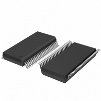
... NXP Semiconductors 13. Package outline TSSOP48: plastic thin shrink small outline package; 48 leads; body width 6 pin 1 index 1 DIMENSIONS (mm are the original dimensions). A UNIT max. 0.15 1.05 mm 1.2 0.25 0.05 0.85 Notes 1. Plastic or metal protrusions of 0.15 mm maximum per side are not included. 2. Plastic interlead protrusions of 0.25 mm maximum per side are not included. ...
Page 36
... NXP Semiconductors 14. Handling information All input and output pins are protected against ElectroStatic Discharge (ESD) under normal handling. When handling Metal-Oxide Semiconductor (MOS) devices ensure that all normal precautions are taken as described in JESD625-A, IEC 61340-5 or equivalent standards. 15. Soldering of SMD packages This text provides a very brief insight into a complex technology. A more in-depth account of soldering ICs can be found in Application Note AN10365 “ ...
Page 37
... NXP Semiconductors 15.3 Wave soldering Key characteristics in wave soldering are: • Process issues, such as application of adhesive and flux, clinching of leads, board transport, the solder wave parameters, and the time during which components are exposed to the wave • Solder bath specifications, including temperature and impurities 15 ...
Page 38
... NXP Semiconductors Fig 26. Temperature profiles for large and small components For further information on temperature profiles, refer to Application Note AN10365 “Surface mount reflow soldering description”. 16. Abbreviations Table 22. Acronym CMOS CDM DC HBM LCD MM MSL PCB RAM RC RMS SCL SDA SMD PCF85162_2 Product data sheet ...
Page 39
... NXP Semiconductors 17. References [1] AN10365 — Surface mount reflow soldering description [2] IEC 60134 — Rating systems for electronic tubes and valves and analogous semiconductor devices [3] IEC 61340-5 — Protection of electronic devices from electrostatic phenomena [4] IPC/JEDEC J-STD-020D — Moisture/Reflow Sensitivity Classification for Nonhermetic Solid State Surface Mount Devices [5] JESD22-A114 — ...
Page 40
... Document ID Release date PCF85162_2 20100507 • Modifications: The format of this data sheet has been redesigned to comply with the new identity guidelines of NXP Semiconductors. • Legal texts have been adapted to the new company name where appropriate. • Corrected ESD values • Added ...
Page 41
... In no event shall NXP Semiconductors be liable for any indirect, incidental, punitive, special or consequential damages (including - without limitation - lost profits, lost savings, business interruption, costs related to the removal or ...
Page 42
... For sales office addresses, please send an email to: PCF85162_2 Product data sheet own risk, and (c) customer fully indemnifies NXP Semiconductors for any liability, damages or failed product claims resulting from customer design and use of the product for automotive applications beyond NXP Semiconductors’ ...
Page 43
... NXP Semiconductors 21. Contents 1 General description . . . . . . . . . . . . . . . . . . . . . . 1 2 Features and benefits . . . . . . . . . . . . . . . . . . . . 1 3 Ordering information . . . . . . . . . . . . . . . . . . . . . 2 4 Marking . . . . . . . . . . . . . . . . . . . . . . . . . . . . . . . . 2 5 Block diagram . . . . . . . . . . . . . . . . . . . . . . . . . . 2 6 Pinning information . . . . . . . . . . . . . . . . . . . . . . 3 6.1 Pinning . . . . . . . . . . . . . . . . . . . . . . . . . . . . . . . 3 6.2 Pin description . . . . . . . . . . . . . . . . . . . . . . . . . 4 7 Functional description . . . . . . . . . . . . . . . . . . . 5 7.1 Power-on reset . . . . . . . . . . . . . . . . . . . . . . . . . 6 7.2 LCD bias generator . . . . . . . . . . . . . . . . . . . . . 6 7.3 LCD voltage selector . . . . . . . . . . . . . . . . . . . . 7 7.4 LCD drive mode waveforms . . . . . . . . . . . . . . . 9 7 ...