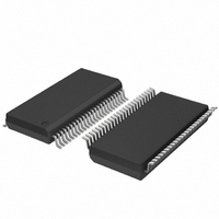
PCF85162T/1,118 NXP Semiconductors, PCF85162T/1,118 Datasheet - Page 17

PCF85162T/1,118
Manufacturer Part Number
PCF85162T/1,118
Description
IC LCD DISPLAY DVR 32SEG 48TSSOP
Manufacturer
NXP Semiconductors
Datasheet
1.PCF85162T1118.pdf
(43 pages)
Specifications of PCF85162T/1,118
Package / Case
48-TSSOP
Display Type
LCD
Configuration
32 Segment
Interface
I²C
Digits Or Characters
Any Digit Type
Current - Supply
8µA
Voltage - Supply
1.8 V ~ 5.5 V
Operating Temperature
-40°C ~ 85°C
Mounting Type
Surface Mount
Number Of Digits
16
Number Of Segments
128
Maximum Clock Frequency
400 KHz
Operating Supply Voltage
1.8 V to 5.5 V
Maximum Power Dissipation
400 mW
Maximum Operating Temperature
+ 85 C
Attached Touch Screen
No
Maximum Supply Current
50 mA
Minimum Operating Temperature
- 40 C
Dc
1123
Lead Free Status / RoHS Status
Lead free / RoHS Compliant
Other names
568-5059-2
NXP Semiconductors
PCF85162_2
Product data sheet
7.12 Subaddress counter
7.11 Data pointer
The following applies to
The addressing mechanism for the display RAM is realized using the data pointer. This
allows the loading of an individual display data byte, or a series of display data bytes, into
any location of the display RAM. The sequence commences with the initialization of the
data pointer by the load-data-pointer command (see
an arriving data byte is stored at the display RAM address indicated by the data pointer.
The filling order is shown in
After each byte is stored, the content of the data pointer is automatically incremented by a
value dependent on the selected LCD drive mode:
If an I
The data pointer should be re-written prior to further RAM accesses.
The storage of display data is determined by the contents of the subaddress counter.
Storage is allowed only when the content of the subaddress counter matches with the
hardware subaddress applied to A0, A1 and A2. The subaddress counter value is defined
by the device-select command (see
and the hardware subaddress do not match then data storage is inhibited but the data
pointer is incremented as if data storage had taken place. The subaddress counter is also
incremented when the data pointer overflows.
In cascaded applications each PCF85162 in the cascade must be addressed separately.
Initially, the first PCF85162 is selected by sending the device-select command matching
the first device's hardware subaddress. Then the data pointer is set to the preferred
display RAM address by sending the load-data-pointer command.
•
•
•
•
•
•
•
•
In static drive mode the eight transmitted data bits are placed in row 0 as one byte.
In 1:2 multiplex drive mode the eight transmitted data bits are placed in pairs into
row 0 and 1 as two successive 4-bit RAM words.
In 1:3 multiplex drive mode the eight bits are placed in triples into row 0, 1, and 2 as
three successive 3-bit RAM words, with bit 3 of the third address left unchanged. It is
not recommended to use this bit in a display because of the difficult addressing. This
last bit may, if necessary, be controlled by an additional transfer to this address but
care should be taken to avoid overwriting adjacent data because always full bytes are
transmitted.
In 1:4 multiplex drive mode, the eight transmitted data bits are placed in quadruples
into row 0, 1, 2, and 3 as two successive 4-bit RAM words.
In static drive mode by eight
In 1:2 multiplex drive mode by four
In 1:3 multiplex drive mode by three
In 1:4 multiplex drive mode by two
2
C-bus data access is terminated early then the state of the data pointer is unknown.
All information provided in this document is subject to legal disclaimers.
Rev. 02 — 7 May 2010
Figure
Figure
11:
11.
Table
12). If the content of the subaddress counter
Universal LCD driver for low multiplex rates
Table
11). Following this command,
PCF85162
© NXP B.V. 2010. All rights reserved.
17 of 43


