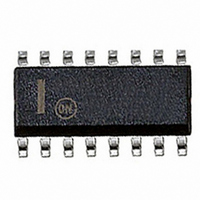
NCP1280DR2 ON Semiconductor, NCP1280DR2 Datasheet - Page 15

NCP1280DR2
Manufacturer Part Number
NCP1280DR2
Description
IC CTRLR PWM PROG OVP HV 16SOIC
Manufacturer
ON Semiconductor
Datasheet
1.NCP1280DR2.pdf
(17 pages)
Specifications of NCP1280DR2
Output Isolation
Isolated
Frequency Range
140 ~ 320kHz
Voltage - Input
7 ~ 25 V
Operating Temperature
-40°C ~ 150°C
Package / Case
16-SOIC (0.154", 3.90mm Width)
Number Of Outputs
Dual Output
Topology
Forward, Half-Bridge
Output Voltage
- 0.3 V to + 18.3 V
Output Current
10 mA
Switching Frequency
315 KHz, 158 KHz
Duty Cycle (max)
80 %
Maximum Operating Temperature
+ 125 C
Minimum Operating Temperature
- 40 C
Fall Time
12 ns
Mounting Style
SMD/SMT
Rise Time
30 ns
Synchronous Pin
No
Lead Free Status / RoHS Status
Contains lead / RoHS non-compliant
Available stocks
Company
Part Number
Manufacturer
Quantity
Price
Part Number:
NCP1280DR2G
Manufacturer:
ON/安森美
Quantity:
20 000
Maximum Duty Cycle
time of OUT1 by comparing the FF Ramp to V
FF Ramp voltage exceeds V
DC Comparator goes high. This will reset the Output Latch,
thus turning OFF the outputs and limiting the duty cycle.
desired DC if the operating frequency is known. The
maximum ON time is set by adjusting the FF Ramp to reach
V
The maximum ON time should be set for the minimum line
voltage. As line voltage increases, the slope of the FF Ramp
increases. This reduces the duty cycle below DC
is a desirable feature as the duty cycle is inversely
proportional to line voltage.
to set V
0.88 V. If the pin is floating, V
equivalent to 60% or 80% of a 1.5 V FF Ramp. V
be adjusted to other values by using an external resistor
network on the DC
line voltage is 100 V, R
is 200 kHz and a maximum duty cycle of 70% is required,
V
from the DC
limit can be disabled connecting a 100 kW resistor between
the DC
Oscillator Ramp
FF Ramp
DC(inv)
DC(inv)
A dedicated internal comparator limits the maximum ON
Duty cycle is defined as:
Therefore, the maximum ON time can be set to yield the
An internal resistor divider from a 2.0 V reference is used
This can be achieved by connecting a 19.6 kW resistor
0 V
0 V
V DC(inv) +
Figure 33. Maximum ON Time Limit Waveforms
MAX
DC(inv)
in a time equal to t
is calculated as follows:
V DC(inv) +
t
on(max)
and V
MAX
. If the DC
T
55.2 mA
REF
pin to GND. The maximum duty cycle
DC +
MAX
10 pF
I FF
pins.
FF
pin. For example, if the minimum
MAX
t on
is 1.82 MW, operating frequency
T
6.7 kW
C FF
on(max)
DC(inv)
+ t on
6.7 kW
pin is grounded, V
125 kW
DC(inv)
, the output of the Max
as shown in Figure 33.
125 kW
3.5 ms
f
t on(max)
is 1.19 V. This is
+1.04 V
DC(inv)
MAX
DC(inv)
DC(inv)
V
, which
http://onsemi.com
. If the
2 V
DC(inv)
can
is
15
5.0 V Reference
The reference output is biased directly from V
supply up to 6 mA. Load regulation is 50 mV and line
regulation is 100 mV over the complete operating range.
0.1 mF ceramic capacitor. The reference output is disabled
when an UV fault is present.
PWM Comparator
duty cycle by comparing the error signal to the FF Ramp.
The error signal is fed into the V
be driven directly with an optocoupler and a pullup resistor
from V
internally incorporating a series diode and resistor. The
series diode provides a 0.7 V offset between V
the PWM comparator inverting input. The outputs are
enabled if the V
valley voltage of the FF Ramp.
the error signal, the voltage on the V
amplitude of the FF Ramp. Otherwise, the converter will not
be able to reach maximum duty cycle. The V
required to control the DC from 0% to DC
the equation below:
where, V
threshold.
Soft−Start
steady state operation, thus reducing startup stress and
surges on the system. The duty cycle is limited during a
soft−start sequence by comparing the Oscillator Ramp to the
SS voltage (V
the SS pin once faults are removed and V
The Soft−Start Comparator controls the duty cycle while the
SS voltage is below 2.0 V. Once V
the Oscillator Ramp voltage and the Soft−Start Comparator
does not limit the duty cycle. Figure 34 shows the
relationship between the outputs duty cycle and the
soft−start voltage.
The NCP1280 includes a precision 5.0 V reference output.
It is recommended to bypass the reference output with a
In steady state operation, the PWM comparator adjusts the
The pullup resistor is selected such that in the absence of
Soft−start (SS) allows the converter to gradually reach
A 6.2 mA current source starts to charge the capacitor on
V EA(L) t V EA t
REF
EA(L)
. The drive of the V
SS
EA
) by means of the Soft−Start Comparator.
is the PWM comparator lower input
voltage is approximately 0.7 above the
186.56 pf
I FF
EA
SS
EA
input. The V
EA
DC
reaches 2.0 V, it exceeds
pin is simplified by
pin exceeds the peak
f
AUX
) V EA(L)
MAX
AUX
reaches 11 V.
EA
EA
is given by
EA
input and
and it can
input can
range


