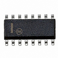
NCP1280DR2 ON Semiconductor, NCP1280DR2 Datasheet - Page 11

NCP1280DR2
Manufacturer Part Number
NCP1280DR2
Description
IC CTRLR PWM PROG OVP HV 16SOIC
Manufacturer
ON Semiconductor
Datasheet
1.NCP1280DR2.pdf
(17 pages)
Specifications of NCP1280DR2
Output Isolation
Isolated
Frequency Range
140 ~ 320kHz
Voltage - Input
7 ~ 25 V
Operating Temperature
-40°C ~ 150°C
Package / Case
16-SOIC (0.154", 3.90mm Width)
Number Of Outputs
Dual Output
Topology
Forward, Half-Bridge
Output Voltage
- 0.3 V to + 18.3 V
Output Current
10 mA
Switching Frequency
315 KHz, 158 KHz
Duty Cycle (max)
80 %
Maximum Operating Temperature
+ 125 C
Minimum Operating Temperature
- 40 C
Fall Time
12 ns
Mounting Style
SMD/SMT
Rise Time
30 ns
Synchronous Pin
No
Lead Free Status / RoHS Status
Contains lead / RoHS non-compliant
Available stocks
Company
Part Number
Manufacturer
Quantity
Price
Part Number:
NCP1280DR2G
Manufacturer:
ON/安森美
Quantity:
20 000
Introduction
improvements and system cost savings over a converter
using a traditional forward topology. The NCP1280
provides two control outputs. OUT1 controls the primary
switch of a forward converter. OUT2 has an adjustable
overlap delay, which can be used to control an active
clamp/reset switch or any other complementary drive
topology, such as an asymmetric half−bridge. In addition,
OUT2 can be used to control a synchronous rectifier
topology, eliminating the need of external control circuitry.
Other distinctive features include: two mode overcurrent
protection, line under/overvoltage detectors, fast line
feedforward, soft−start and a maximum duty cycle limit.
The Functional Block Diagram is shown in Figure 2.
the advantages of Current−Mode Control, such as fast line
feedforward, and cycle by cycle current limit. It eliminates
the disadvantages of low power jitter, slope compensation
and noise susceptibility.
Active Clamp Topology
converter is set by the turns ratio and input voltage. Where
as the reset voltage of an active clamp topology is constant
over the converter off time and only depends on the input
voltage and duty cycle. This translates into a lower voltage
stress on the main switch, allowing the use of lower voltage
MOSFETs. In general, lower voltage MOSFETs have lower
cost and ON resistance. Therefore, lower system cost and
higher efficiency can be achieved. In addition, the lower
voltage stress allows the converter to operate at a higher duty
cycle for a given primary switch voltage stress. This allows
a reduction in primary peak current and secondary side
voltage stress as well as smaller secondary inductor size.
An NCP1280 based system offers significant efficiency
The features included in the NCP1280 provide some of
The transformer reset voltage in a traditional forward
80
70
60
50
40
30
20
10
0
0
Measured from 10% to 90% of V
V
AUX
Figure 27. Outputs Rise Time versus Load
25
= 12 V
50
C
L
, LOAD CAPACITANCE (pF)
75
Capacitance
T
J
= 25°C
100
OH
125
DETAILED OPERATING DESCRIPTION
T
J
T
= −40°C
TYPICAL CHARACTERISTICS
J
150
= 125°C
175
http://onsemi.com
200
11
High Voltage Startup Regulator
that eliminates the need for external startup components. In
addition, this regulator increases the efficiency of the supply
as it uses no power when in the normal mode of operation,
but instead uses power supplied by an auxiliary winding.
that supplies current from the input line voltage (V
capacitor on the V
typically 13.8 mA. Once V
regulator turns OFF and the outputs are enabled. When V
reaches 7 V, the outputs are disabled and the startup regulator
turns ON. This “7−11” mode of operation is known as
Dynamic Self Supply (DSS). The V
externally above 7 V once the outputs are enabled to prevent
the startup regulator from turning ON. It is recommended to
bias the V
auxiliary winding from the power transformer. An
independent voltage supply can also be used. If using an
independent voltage supply and V
outputs are enabled or while a fault is present, the One Shot
Pulse Generator (Figure 2) will not be enabled and the
outputs will remain OFF.
be placed between C
in Figure 29. This will allow the NCP1280 to charge C
while preventing the startup regulator from sourcing current
into the auxiliary supply.
35
30
25
20
15
10
The NCP1280 contains an internal 700 V startup regulator
The startup regulator consists of a constant current source
As the DSS sources current to the V
5
0
0
Measured from 90% to 10% of V
V
AUX
Figure 28. Outputs Fall Time versus Load
AUX
25
= 12 V
pin using an auxiliary supply generated by an
C
50
L
AUX
, LOAD CAPACITANCE (pF)
AUX
75
pin (C
Capacitance
and the auxiliary supply as shown
AUX
100
AUX
T
J
reaches 11 V, the startup
= 125°C
T
AUX
). The startup current is
OH
J
125
AUX
AUX
= 25°C
is biased before the
pin, a diode should
pin can be biased
150
T
J
= −40°C
175
in
) to the
AUX
AUX
200


