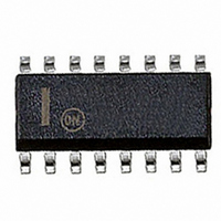
NCP1280DR2 ON Semiconductor, NCP1280DR2 Datasheet

NCP1280DR2
Specifications of NCP1280DR2
Available stocks
Related parts for NCP1280DR2
NCP1280DR2 Summary of contents
Page 1
... DC SS MAX ORDERING INFORMATION See detailed ordering and shipping information in the package dimensions section on page 4 of this data sheet. *For additional information on our Pb−Free strategy and soldering details, please download the ON Semiconductor Soldering and Mounting Techniques Reference Manual, SOLDERRM/D. L out out out − ...
Page 2
V in Disable I START 16 V AUX C AUX + AUX(ON) AUX(OFF) − GND Disable_V − 1.49 V − 3 UV/OV + − + 3.6 V − V REF Disable − ...
Page 3
PIN DESCRIPTION Pin Name 1 V This pin is connected to the input voltage of the system. The voltage can be a rectified, filtered line voltage in or output of a power factor correction (PFC) front end. A constant current ...
Page 4
... ORDERING INFORMATION Device NCP1280DR2G †For information on tape and reel specifications, including part orientation and tape sizes, please refer to our Tape and Reel Packaging Specifications Brochure, BRD8011/D. MAXIMUM RATINGS (Note 1) Rating Input Line Voltage Auxiliary Supply Voltage Transient Auxiliary Supply Voltage (Duration < 10 ms, I ...
Page 5
ELECTRICAL CHARACTERISTICS R = 60.4 kW 1.0 MW, for typical values Characteristic STARTUP CONTROL AND V REGULATOR AUX V Regulation AUX Startup Threshold/V Regulation Peak (V AUX Minimum Operating V Valley Voltage After Turn−On AUX ...
Page 6
ELECTRICAL CHARACTERISTICS R = 60.4 kW 1.0 MW, for typical values Characteristic OSCILLATOR Frequency (R = 101 kW 25° −40°C to 125°C J Frequency (R = 220 kW, V ...
Page 7
STARTUP THRESHOLD MINIMUM OPERATING 6 THRESHOLD 5 −50 − JUNCTION TEMPERATURE (°C) J Figure 3. Auxiliary Supply Voltage Thresholds versus Junction Temperature 17.0 16.5 16.0 15.5 15.0 14.5 ...
Page 8
OSC −50 − JUNCTION TEMPERATURE (°C) J Figure 9. Operating Auxiliary Supply Current versus Junction Temperature 160 150 OV HYSTERESIS 140 ...
Page 9
T , JUNCTION TEMPERATURE (°C) J Figure 15. Oscillator Frequency versus Junction Temperature −50 −25 0 ...
Page 10
T , JUNCTION TEMPERATURE (°C) J Figure 21. V Input Resistance versus EA Junction Temperature 5.03 5. REF 4. REF ...
Page 11
Measured from 10 AUX T = 25° 100 C , LOAD CAPACITANCE (pF) L Figure 27. Outputs Rise ...
Page 12
I START I START V V AUX in I AUX C AUX Disable Figure 29. Recommended V AUX Power to the controller while operating in the self−bias or DSS mode is provided Therefore, C AUX sized such ...
Page 13
V AUX(on) V AUX V AUX(off UV/OV Voltage 0 V Soft−Start Voltage 0 V OUT2 0 V OUT1 0 V Figure 31. Soft−Start Timing Diagram (Using Auxiliary Winding) Feedforward Ramp Generator The NCP1280 incorporates line feedforward ...
Page 14
Current Limit The NCP1280 has two overcurrent protection modes, cycle by cycle and cycle skip. It allows the NCP1280 to handle momentary and hard shorts differently for the best tradeoff in performance and safety. The outputs are disabled typically 90 ...
Page 15
Maximum Duty Cycle A dedicated internal comparator limits the maximum ON time of OUT1 by comparing the FF Ramp Ramp voltage exceeds V , the output of the Max DC(inv) DC Comparator goes high. This will reset ...
Page 16
... If the control outputs need to drive a large capacitive load, a driver should be used between the NCP1280 and the load. ON Semiconductor’s MC33152 is a good selection for an integrated driver. Figures 27 and 28 shows the relationship between the output’s rise and fall times vs capacitive load. ...
Page 17
... Opportunity/Affirmative Action Employer. This literature is subject to all applicable copyright laws and is not for resale in any manner. PUBLICATION ORDERING INFORMATION LITERATURE FULFILLMENT: Literature Distribution Center for ON Semiconductor P.O. Box 5163, Denver, Colorado 80217 USA Phone: 303−675−2175 or 800−344−3860 Toll Free USA/Canada Fax: 303− ...


