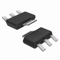
NCP1015ST100T3G ON Semiconductor, NCP1015ST100T3G Datasheet - Page 3

NCP1015ST100T3G
Manufacturer Part Number
NCP1015ST100T3G
Description
IC OFFLINE SWIT SMPS CM SOT223
Manufacturer
ON Semiconductor
Datasheet
1.NCP1015ST100T3G.pdf
(22 pages)
Specifications of NCP1015ST100T3G
Output Isolation
Isolated
Frequency Range
90 ~ 110kHz
Voltage - Input
8.5 ~ 10 V
Voltage - Output
700V
Power (watts)
19W
Operating Temperature
0°C ~ 150°C
Package / Case
TO-261-4, TO-261AA, SOT-223-4
Duty Cycle (max)
72 %
Mounting Style
SMD/SMT
Switching Frequency
1000 KHz
Operating Supply Voltage
- 0.3 V to + 10 V
Maximum Operating Temperature
+ 150 C
Minimum Operating Temperature
- 60 C
Operating Temperature (max)
150C
Pin Count
3 +Tab
Mounting
Surface Mount
Package Type
SOT-223
Case Length
6.5mm
Case Height
1.57mm
Lead Free Status / RoHS Status
Lead free / RoHS Compliant
Available stocks
Company
Part Number
Manufacturer
Quantity
Price
Part Number:
NCP1015ST100T3G
Manufacturer:
ON/安森美
Quantity:
20 000
Stresses exceeding Maximum Ratings may damage the device. Maximum Ratings are stress ratings only. Functional operation above the
Recommended Operating Conditions is not implied. Extended exposure to stresses above the Recommended Operating Conditions may affect
device reliability.
GND
V
MAXIMUM RATINGS
NC
FB
CC
1
2
3
4
Symbol
TJ
I_V
Ids
R
R
R
R
V
Vds
qJA
qJA
MAX
CC
qJL
qJL
CC
4 V
pk
18 k
V
CC
Power Supply voltage on all pins, except pin 5 (drain)
Drain voltage
Drain peak current during transformer saturation
Maximum current into pin 1
Maximum Junction Temperature
Storage Temperature Range
ESD Capability, Human Body Model (HBM) (All pins except HV)
ESD Capability, Machine Model (MM)
Error flag armed?
Thermal Characteristics
P Suffix, Case 626A
ST Suffix, Plastic Package Case 318E
Junction−to−Lead
Junction−to−Air, 2.0 oz (70 mm) Printed Circuit Copper Clad
Junction−to−Lead
Junction−to−Air, 2.0 oz (70 mm) Printed Circuit Copper Clad
0.36 Sq. Inch (2.32 Sq. Cm)
1.0 Sq. Inch (6.45 Sq. Cm)
0.36 Sq. Inch (2.32 Sq. Cm)
1.0 Sq. Inch (6.45 Sq. Cm)
Startup Source
Management
EMI Jittering
UVLO
Overload?
Figure 2. Simplified Internal Circuit Architecture
High when V
Drain
http://onsemi.com
100 kHz
65 kHz
Clock
Rating
CC
0.5 V
Soft−Start
t 3 V
3
−
+
Set
D
Startup Sequence
Overload
Flip−Flop
max
Reset
Reset
= 65%
Q
Driver
V
-
+
CC
250 ns
L.E.B.
−60 to +150
−0.3 to 700
−0.3 to 10
Value
Drain
150
200
9.0
15
77
60
14
74
55
R
1
2
sense
°C/W
Unit
mA
8
7
5
°C
°C
kV
V
V
A
V
DRAIN
GND
GND


