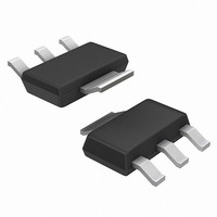
NCP1015ST100T3G ON Semiconductor, NCP1015ST100T3G Datasheet - Page 14

NCP1015ST100T3G
Manufacturer Part Number
NCP1015ST100T3G
Description
IC OFFLINE SWIT SMPS CM SOT223
Manufacturer
ON Semiconductor
Datasheet
1.NCP1015ST100T3G.pdf
(22 pages)
Specifications of NCP1015ST100T3G
Output Isolation
Isolated
Frequency Range
90 ~ 110kHz
Voltage - Input
8.5 ~ 10 V
Voltage - Output
700V
Power (watts)
19W
Operating Temperature
0°C ~ 150°C
Package / Case
TO-261-4, TO-261AA, SOT-223-4
Duty Cycle (max)
72 %
Mounting Style
SMD/SMT
Switching Frequency
1000 KHz
Operating Supply Voltage
- 0.3 V to + 10 V
Maximum Operating Temperature
+ 150 C
Minimum Operating Temperature
- 60 C
Operating Temperature (max)
150C
Pin Count
3 +Tab
Mounting
Surface Mount
Package Type
SOT-223
Case Length
6.5mm
Case Height
1.57mm
Lead Free Status / RoHS Status
Lead free / RoHS Compliant
Available stocks
Company
Part Number
Manufacturer
Quantity
Price
Part Number:
NCP1015ST100T3G
Manufacturer:
ON/安森美
Quantity:
20 000
current flowing through R
the V
is fired. The NPN base can also receive a signal from a
temperature sensor. Typical bipolar can be MMBT2222 and
MMBT2907 for the discrete latch. The NST3946 features
two bipolar NPN + PNP in the same package and could also
be used.
Power Dissipation and Heatsinking
dissipation DSS current−source (when active) and the
dissipation of MOSFET. Thus P
When the PDIP7 package is surrounded by copper, it
becomes possible to drop its thermal resistance
junction−to−ambient, R
dissipate more power. The maximum power the device can
thus evacuate is:
Design Procedure
not differ from that of a standard circuit using a controller
and a MOSFET. However, one needs to be aware of certain
characteristics specific of monolithic devices:
R
The power dissipation of NCP1015 consists of the
The design of a SMPS around a monolithic device does
hold
CC
ensures that the SCR stays on when fired. The bias
ramp up (8.5 V) and down (7.5 V) when the SCR
Figure 24. A Possible PCB Arrangement to Reduce the Thermal Resistance Junction−to−Ambient
Figure 23. Two Bipolar Transistors Ensures a Total Latch−off of the SMPS in Presence of an OVP
0.1 mF
OVP
qJA
hold
DC
down to 75°C/W and thus
should be small enough to let
10 k
tot
= P
10 k
DSS
+ P
BAT54
Rhold
12 k
Clamping Elements
MOSFET
http://onsemi.com
.
14
which gives around 1 W for an ambient of 50°C. The losses
inherent to the MOSFET R
following formula:
where I
input), D is the converter operating duty−cycle and R
the MOSFET resistance for T
valid for Discontinuous Conduction Mode (DCM)
operation where the turn−on losses are null (the primary
current is zero when you re−start the MOSFET). Figure 24
gives a possible layout to help dropping the thermal
resistance. When measured on a 35 mm (1 oz.) copper
thickness PCB, we obtained a thermal resistance of 75°C/W:
+
CV
CC
1. In any case, the lateral MOSFET body−diode shall
never be forward biased, either during start−up
(because of a large leakage inductance) or in
normal operation as shown by Figure 25.
p
1
2
3
4
is the worse case peak current (at the lowest line
P
P
mos
max
+
+ 1
8
7
5
3
T
J(max)
@ I
To Secondary Diode
DS(on)
p
J
2
= 100°C. This formula is only
@ D @ R
Transformer
* T
R
qJA
can be evaluated using the
AMB(max)
DS(on)
(eq. 12)
(eq. 13)
DS(on)


