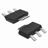
NCP1015ST100T3G ON Semiconductor, NCP1015ST100T3G Datasheet - Page 16

NCP1015ST100T3G
Manufacturer Part Number
NCP1015ST100T3G
Description
IC OFFLINE SWIT SMPS CM SOT223
Manufacturer
ON Semiconductor
Datasheet
1.NCP1015ST100T3G.pdf
(22 pages)
Specifications of NCP1015ST100T3G
Output Isolation
Isolated
Frequency Range
90 ~ 110kHz
Voltage - Input
8.5 ~ 10 V
Voltage - Output
700V
Power (watts)
19W
Operating Temperature
0°C ~ 150°C
Package / Case
TO-261-4, TO-261AA, SOT-223-4
Duty Cycle (max)
72 %
Mounting Style
SMD/SMT
Switching Frequency
1000 KHz
Operating Supply Voltage
- 0.3 V to + 10 V
Maximum Operating Temperature
+ 150 C
Minimum Operating Temperature
- 60 C
Operating Temperature (max)
150C
Pin Count
3 +Tab
Mounting
Surface Mount
Package Type
SOT-223
Case Length
6.5mm
Case Height
1.57mm
Lead Free Status / RoHS Status
Lead free / RoHS Compliant
Available stocks
Company
Part Number
Manufacturer
Quantity
Price
Part Number:
NCP1015ST100T3G
Manufacturer:
ON/安森美
Quantity:
20 000
with V
DCM operation is lost, there is another expression we can
write to connect L
NCP1015 and the maximum duty−cycle that needs to stay
below 50%:
MOSFET:
the MOSFET:
to which switching losses shall be added.
above calculations, we will discover that a power supply
built with the NCP1015 and operating from a 100 Vac line
minimum will not be able to deliver more than 7 W
continuous, regardless of the selected switching frequency
(however the transformer core size will go down as f
increased). This number grows up significantly when
operated from single European mains (18 W).
examples we recommend use following support:
capability of the NCP101X members”
with the NCP101X members.”
mains adapter with NCP101X series”.
Example 1.: A 12 V 7.0 W SMPS Operating on a Large
Mains with NCP1015:
V
rectified, assuming a low bulk ripple
Efficiency = 80%
V
f
I
sw
P(max)
out
in
If L
From Equation 22 we obtain the operating duty−cycle D:
This lets us calculate the RMS current circulating in the
From this equation, we obtain the average dissipation in
If we stick to Equation 23, compute Lp and follow the
For more different flyback converters then are the below
1) Application note AND8125/D “Evaluating the power
2) Application note AND8134/D “Designing Converters
3) Application note AND8142/D “A 6W/12W Universal
4) The PSpice or Orcad simulation models
= 65 kHz
= 100 Vac ÷ 250 Vac or 140 Vdc ÷ 350 Vdc once
= 12 V, I
p
r
= 450 mA − 10% = 405 mA
= N . (V
critical gives the inductance value above which
out
L
P
P(max)
P
max
out
= 580 mA
avg
p
, the primary peak current bounded by the
+ V
+ t
I
+ 1
D(rms)
+
D +
f
3
sw
) and h the efficiency.
D
@ I
2
max
@ V
+ I
V
p
I
2
in
p
L
@ V
@ D @ R
@ L
IN(min)
p
@ t
Pcritical
I
P(max)
@
sw
IN(min)
p
D
2
3
DS(on)
+
@ V
@ t
2 @ f
r
sw
2
@ h @
sw
@ [P
(2L
(eq. 22)
(eq. 24)
(eq. 25)
(eq. 26)
out
http://onsemi.com
P(max)
sw
@ (V
(V
is
in
V
r
r
@ V
2
2
16
) 2 @ V
) 4L
r
)
2
where V
hence the longest ton duration or largest duty−cycle. I
is the available peak current from the considered part, e.g.
450 mA typical for the NCP1015 (however, the minimum
value of this parameter shall be considered for reliable
evaluation). Combining Equations 21 and 22 gives the
maximum theoretical power you can pass respecting the
peak current capability of the NCP1015, the maximum
duty−cycle and the discontinuous mode operation:
Applying the above equations leads to :
Selected maximum reflected voltage = 120 V
with V
L
I
D
I
P
P
Secondary diode voltage stress = (350 x 0.1) + 12 = 47 V
(e.g. a MBRS360T3, 3 A / 60 V would fit)
Example 2.: A 12 V 16 W SMPS Operating on Narrow
European Mains with NCP1015:
V
Efficiency = 80%
V
f
I
Selected maximum reflected voltage = 250 V
with V
L
I
D
I
P
P
ambient of 50°C.
Secondary diode voltage stress = (370 x 0.05) + 12 = 30.5 V
(e.g. a MBRS340T3, 3 A / 40 V)
p
DRAIN(rms)
sw
P(max)
p
DRAIN(rms)
@ h
MOSFET
DSS
MOSFET
DSS
p
out
p
in
max
max
Applying the equations leads to :
P(max)
= 250 mA
= 0.27 mA
critical = 3.9 mH
= 7,2 mH
= 65 kHz
= 230 Vac ± 15%, or 276 Vdc ÷ 370 Vdc
r
= 12 V, I
@ V
f
= 1.2 mA x 350 V = 420 mW, if DSS is used
= 1.2 mA x 370 V = 444 mW, if DSS is used below an
= 0.39
= 0.41
sw
out
out
= 450 mA − 10% = 405 mA
V
in
IN(min)
r
= 12 V, secondary drop = 0.5 V ³ Np : Ns = 1 : 0.1
= 12 V, secondary drop = 0.5 V ³ Np : Ns = 1:0.05
= 202 mW at R
= 250 mW at R
V
) V
IN(min)
= 90 mA
= 100 mA
out
in
2
= 1.25 A
corresponds to the lowest bulk voltage,
)]
) V
(eq. 21)
IN(min)
DS(on)
DS(on)
2
)
(eq. 23)
= 25 W (T
= 25 W (T
J
J
> 100°C)
> 100°C)
P(max)


