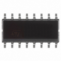
L6566B STMicroelectronics, L6566B Datasheet - Page 35

L6566B
Manufacturer Part Number
L6566B
Description
IC CTRLR OVP OTP UVLO HV 16SOIC
Manufacturer
STMicroelectronics
Datasheet
1.L6566BTR.pdf
(51 pages)
Specifications of L6566B
Output Isolation
Isolated
Frequency Range
10 ~ 300kHz
Voltage - Input
8 ~ 23 V
Power (watts)
750mW
Operating Temperature
-40°C ~ 150°C
Package / Case
16-SOIC (0.154", 3.90mm Width)
Output Current
800 mA
Output Power
750 mW
Input Voltage
8 V to 23 V
Operating Temperature Range
- 40 C to + 150 C
Mounting Style
SMD/SMT
Duty Cycle (max)
75 %
Selectable Multi-mode Operation
fixed frequency or quasi-resonant
For Use With
497-6452 - BOARD EVAL FOR L6566B497-6451 - BOARD EVAL FOR L6566B497-6450 - BOARD EVAL FOR L6566B497-6449 - BOARD EVAL FOR L6566A
Lead Free Status / RoHS Status
Lead free / RoHS Compliant
Available stocks
Company
Part Number
Manufacturer
Quantity
Price
Part Number:
L6566B
Manufacturer:
ST
Quantity:
20 000
Part Number:
L6566BHTR
Manufacturer:
ST
Quantity:
20 000
Part Number:
L6566BTR-13
Manufacturer:
ST
Quantity:
20 000
L6566B
5.11
OVP block
The OVP function of the L6566B monitors the voltage on the ZCD pin (11) in MOSFET’s
OFF-time, during which the voltage generated by the auxiliary winding tracks converter’s
output voltage. If the voltage on the pin exceeds an internal 5 V reference, a comparator is
triggered, an overvoltage condition is assumed and the device is shut down. An internal
current generator is activated that sources 1 mA out of the VFF pin (15). If the VFF voltage
is allowed to reach 2 Vbe over 5 V, the L6566B will be latched off. See
disable function on page 32
impedance externally connected to pin 15 is so low that the 5+2 V
reached or if some means is provided to prevent that, the device will be able to restart after
the Vcc has dropped below 5 V. Refer to the “Application examples and Ideas” section
(
Figure 22. OVP function: internal block diagram
The ZCD pin will be connected to the auxiliary winding through a resistor divider R
(see
to:
Equation 13
where Vout
number of the secondary winding and Naux the turn number of the auxiliary winding.
Table 7 on page 45
Figure 8 on page 20
PWM latch
R
S
Q
Q
OVP
is the output voltage value that is to activate the protection, Ns the turn
) for additional hints.
Monostable
M1
to triggering
). The divider ratio k
block
for more details on IC’s behavior under these conditions. If the
2 µs
k
OVP
ZCD
40k Ω
5pF
11
=
Vout
5 V
Monostable
OVP
5
M2
OVP
+
-
= R
STROBE
Naux
Ns
Z2
0.5 µs
COUT
/ (R
Z1
+ R
OVP
R Q1
S
FF
Z2
BE
Application information
) will be chosen equal
threshold cannot be
Section 5.9: Latched
L6566B
counter
2-bit
Counter
reset
Z1
Fault
, R
35/51
Z2


