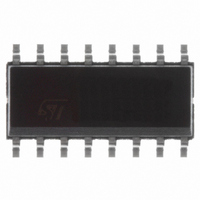
L6566B STMicroelectronics, L6566B Datasheet - Page 10

L6566B
Manufacturer Part Number
L6566B
Description
IC CTRLR OVP OTP UVLO HV 16SOIC
Manufacturer
STMicroelectronics
Datasheet
1.L6566BTR.pdf
(51 pages)
Specifications of L6566B
Output Isolation
Isolated
Frequency Range
10 ~ 300kHz
Voltage - Input
8 ~ 23 V
Power (watts)
750mW
Operating Temperature
-40°C ~ 150°C
Package / Case
16-SOIC (0.154", 3.90mm Width)
Output Current
800 mA
Output Power
750 mW
Input Voltage
8 V to 23 V
Operating Temperature Range
- 40 C to + 150 C
Mounting Style
SMD/SMT
Duty Cycle (max)
75 %
Selectable Multi-mode Operation
fixed frequency or quasi-resonant
For Use With
497-6452 - BOARD EVAL FOR L6566B497-6451 - BOARD EVAL FOR L6566B497-6450 - BOARD EVAL FOR L6566B497-6449 - BOARD EVAL FOR L6566A
Lead Free Status / RoHS Status
Lead free / RoHS Compliant
Available stocks
Company
Part Number
Manufacturer
Quantity
Price
Part Number:
L6566B
Manufacturer:
ST
Quantity:
20 000
Part Number:
L6566BHTR
Manufacturer:
ST
Quantity:
20 000
Part Number:
L6566BTR-13
Manufacturer:
ST
Quantity:
20 000
Pin settings
10/51
Table 1.
N°
11
12 MODE/SC
13
14
15
16
AC_OK
OSC
ZCD
VFF
Pin
SS
Pin functions (continued)
Transformer demagnetization sensing input for quasi-resonant operation and OVP
input. The pin is externally connected to the transformer’s auxiliary winding through
a resistor divider. A negative-going edge triggers MOSFET’s turn-on if QR mode is
selected.
A voltage exceeding 5 V shuts the IC down and brings its consumption to a lower
value (OVP). Latch-off or auto-restart mode is selectable externally. This function is
strobed and digitally filtered to increase noise immunity.
Operating mode selection. If the pin is connected to the VREF pin (7)
quasi-resonant operation is selected, the oscillator (pin 13, OSC) determines the
maximum allowed operating frequency.
Fixed-frequency operation is selected if the pin is not tied to VREF, in which case
the oscillator determines the actual operating frequency, the maximum allowed
duty cycle is set at 70 % min. and the pin delivers a voltage ramp synchronized to
the oscillator when the gate-drive output is high; the voltage delivered is zero while
the gate-drive output is low. The pin is to be connected to pin CS (7) via a resistor
for slope compensation.
Oscillator pin. The pin is an accurate 1 V voltage source, and a resistor connected
from the pin to GND (pin 3) defines a current. This current is internally used to set
the oscillator frequency that defines the maximum allowed switching frequency of
the L6566B, if working in QR mode, or the operating switching frequency if working
in FF mode.
Soft-start current source. At start-up a capacitor Css between this pin and GND
(pin 3) is charged with an internal current generator. During the ramp, the internal
reference clamp on the current sense pin (7, CS) rises linearly starting from zero to
its final value, thus causing the duty cycle to increase progressively starting from
zero as well. During soft-start the adaptive UVLO function and all functions
monitoring pin COMP are disabled. The soft-start capacitor is discharged whenever
the supply voltage of the IC falls below the UVLO threshold. The same capacitor is
used to delay IC’s shutdown (latch-off or auto-restart mode selectable) after
detecting an overload condition (OLP).
Line voltage feedforward input. The information on the converter’s input voltage is
fed into the pin through a resistor divider and is used to change the setpoint of the
pulse-by-pulse current limitation (the higher the voltage, the lower the setpoint).
The linear dynamics of the pin ranges from 0 to 3 V. A voltage higher than 3 V
makes the IC stop switching. If feedforward is not desired, tie the pin to GND (pin 3)
directly if a latch-mode OVP is not required (see pin 11, ZCD) or through a 10 kΩ
min. resistor if a latch-mode OVP is required. Bypass the pin with a capacitor to
GND (pin 3) to reduce noise pick-up.
Brownout protection input. A voltage below 0.45 V shuts down (not latched) the IC,
lowers its consumption and clears the latch set by latched protections (DIS > 4.5 V,
SS > 6.4 V, VFF > 6.4 V). IC’s operation is re-enabled as the voltage exceeds
0.45 V. The comparator is provided with current hysteresis: an internal 15 µA
current generator is ON as long as the voltage on the pin is below 0.45 V and is
OFF if this value is exceeded. Bypass the pin with a capacitor to GND (pin 3) to
reduce noise pick-up. Tie to Vcc with a 220 to 680 kΩ resistor if the function is not
used.
Function
L6566B


