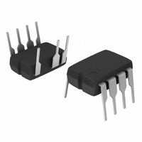
NCP1216AP100G ON Semiconductor, NCP1216AP100G Datasheet - Page 9

NCP1216AP100G
Manufacturer Part Number
NCP1216AP100G
Description
IC CTRLR PWM CM OTP HV 8DIP
Manufacturer
ON Semiconductor
Datasheet
1.NCP1216AP100G.pdf
(18 pages)
Specifications of NCP1216AP100G
Output Isolation
Isolated
Frequency Range
90 ~ 110kHz
Voltage - Input
10 ~ 16 V
Operating Temperature
0°C ~ 150°C
Package / Case
8-DIP (0.300", 7.62mm), 7 Leads
Duty Cycle (max)
50 %
Mounting Style
Through Hole
Switching Frequency
110 KHz
Maximum Operating Temperature
+ 150 C
Fall Time
20 ns
Rise Time
60 ns
Synchronous Pin
No
Topology
Flyback
Lead Free Status / RoHS Status
Lead free / RoHS Compliant
Available stocks
Company
Part Number
Manufacturer
Quantity
Price
Company:
Part Number:
NCP1216AP100G
Manufacturer:
ON Semiconductor
Quantity:
1 700
Part Number:
NCP1216AP100G
Manufacturer:
ON/安森美
Quantity:
20 000
Introduction
architecture where the switch−off event is dictated by the
peak current setpoint. This component represents the ideal
candidate where low part count is the key parameter,
particularly in low−cost AC−DC adapters, TV power
supplies etc. Due to its high−performance High−Voltage
technology, the NCP1216 incorporates all the necessary
components normally needed in UC384X based supplies:
timing components, feedback devices, low−pass filter and
self−supply. This later point emphasizes the fact that ON
Semiconductor’s NCP1216 does NOT need an auxiliary
winding to operate: the product is naturally supplied from
the high−voltage rail and delivers a V
system is called the Dynamic Self−Supply (DSS):
Dynamic Self−Supply (DSS): Due to its Very High
Voltage
ON Semiconductor’s NCP1216 allows for a direct pin
connection to the high−voltage DC rail. A dynamic current
source charges up a capacitor and thus provides a fully
independent V
no need for an auxiliary winding whose management is
always a problem in variable output voltage designs (e.g.
battery chargers).
Adjustable Skip Cycle Level: By offering the ability to tailor
the level at which the skip cycle takes place, the designer can
make sure that the skip operation only occurs at low peak
current. This point guarantees a noise−free operation with
cheap transformers. Skip cycle offers a proven mean to
reduce the standby power in no or light loads situations.
Internal Frequency Dithering for Improved EMI
Signature: By modulating the internal switching frequency
with the DSS V
softens the controller’s EMI signature.
Wide Switching − Frequency Offered with Different
Options (65 kHz − 100 kHz − 133 kHz): Depending on the
application, the designer can pick up the right device to help
reducing magnetics or improve the EMI signature before
reaching the 150 kHz starting point.
Ramp Compensation: By inserting a resistor between the
Current Sense (CS) pin and the actual sense resistor, it
becomes possible to inject a given amount of ramp
compensation since the internal sawtooth clock is routed to
the CS pin. Sub−harmonic oscillations in Continuous
Conduction Mode (CCM) can thus be compensated via a
single resistor.
The NCP1216 implements a standard current mode
Integrated
CC
CC
level to the NCP1216. As a result, there is
ripple, natural energy spread appears and
Circuit
(VHVIC)
CC
to the IC. This
APPLICATION INFORMATION
technology,
http://onsemi.com
9
Over Current Protection (OCP): By continuously
monitoring the FB line activity, NCP1216 enters burst mode
as soon as the power supply undergoes an overload. The
device enters a safe low power operation, which prevents
from any lethal thermal runaway. As soon as the default
disappears, the power supply resumes operation. Unlike
other controllers, overload detection is performed
independently of any auxiliary winding level. In presence of
a bad coupling between both power and auxiliary windings,
the short circuit detection can be severely affected. The DSS
naturally shields you against these troubles.
Wide Duty− Cycle Operation: Wide mains operation requires
a large duty−cycle excursion. The NCP1216 can go up to 75%
typically. For Continuous Conduction Mode (CCM)
applications, the internal ramp compensation lets you fight
against sub−harmonic oscillations.
Low Standby Power: If SMPS naturally exhibit a good
efficiency at nominal load, they begin to be less efficient
when the output power demand diminishes. By skipping
unnecessary switching cycles, the NCP1216 drastically
reduces the power wasted during light load conditions. In
no−load conditions, the NPC1216 allows the total standby
power to easily reach next International Energy Agency
(IEA) recommendations.
No Acoustic Noise While Operating: Instead of skipping
cycles at high peak currents, the NCP1216 waits until the
peak current demand falls below a user−adjustable 1/3 of the
maximum limit. As a result, cycle skipping can take place
without having a singing transformer, one can thus select
cheap magnetic components free of noise problems.
External MOSFET Connection: By leaving the external
MOSFET external to the IC, you can select avalanche proof
devices, which in certain cases (e.g. low output powers), let
you work without an active clamping network. Also, by
controlling the MOSFET gate signal flow; you have an
option to slow down the device commutation, therefore
reducing the amount of ElectroMagnetic Interference
(EMI).
SPICE Model: A dedicated model to run transient
cycle−by−cycle simulations is available but also an
averaged version to help you closing the loop.
Ready−to−use templates can be downloaded in OrCAD’s
PSpice and INTUSOFT’s IsSpice from ON Semiconductor
web site, in the NCP1216 related section.


