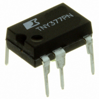
TNY377PN Power Integrations, TNY377PN Datasheet - Page 8

TNY377PN
Manufacturer Part Number
TNY377PN
Description
IC OFFLINE SWIT OVP OTP HV 8DIP
Manufacturer
Power Integrations
Series
TinySwitch®-PKr
Type
Off Line Switcherr
Datasheet
1.TNY376PN.pdf
(22 pages)
Specifications of TNY377PN
Output Isolation
Isolated
Frequency Range
132 ~ 280kHz
Voltage - Output
700V
Power (watts)
28W
Operating Temperature
-40°C ~ 150°C
Package / Case
8-DIP (0.300", 7.62mm), 7 Leads
Output Voltage
700 V
Input / Supply Voltage (max)
9 V
Input / Supply Voltage (min)
- 0.3 V
Duty Cycle (max)
65 %
Switching Frequency
264 KHz
Supply Current
570 uA
Operating Temperature Range
- 40 C to + 150 C
Mounting Style
Through Hole
Maximum Operating Temperature
+ 150 C
Minimum Operating Temperature
- 40 C
Output Current
1.4 A
Output Power
28 W
Lead Free Status / RoHS Status
Lead free / RoHS Compliant
Other names
596-1144-5
Available stocks
Company
Part Number
Manufacturer
Quantity
Price
Company:
Part Number:
TNY377PN
Manufacturer:
POWER
Quantity:
15 000
Figure 14. TNY376PN, Four Output, 7.5 W, 13 W Peak Universal Input Power Supply.
Rev. C 07/09
Applications Examples
The circuit shown in Figure 14 is a low cost universal AC input,
four-output fl yback power supply utilizing a TNY376. The
continuous output power is 7.5 W with a peak of 13 W. The
output voltages are 3.3 V, 5 V, 12 V, and –12 V.
The rectifi ed and fi ltered input voltage is applied to the primary
winding of T1. The other side of the transformer’s primary is
driven by the integrated MOSFET in U1. Diode D5, C3, R1, R2,
and VR1 compose the clamp circuit, limiting the leakage
inductance turn-off voltage spike on the DRAIN pin to a safe
value. The use of a combination Zener clamp and parallel RC
optimizes both EMI and energy effi ciency.
Both the 3.3 V and 5 V outputs are sensed through resistors R6
and R7. The voltage across R8 is regulated to 2.5 V by reference
IC U3. If the voltage across R8 begins to exceed 2.5 V, then
current will fl ow in the LED inside the optocoupler U2, driven by
the cathode of U3. This will cause the transistor of the
optocoupler to sink current from the EN/UV pin of U1. When the
current exceeds the ENABLE pin threshold current, the next
switching cycle is inhibited. Conversely, when the voltage across
resistor R8 falls below 2.5 V, and the current out of the ENABLE
pin is below the threshold, a conduction cycle is allowed to
occur. By adjusting the number of enabled cycles, regulation is
maintained. As the load reduces, the number of enabled cycles
decreases, lowering the effective switching frequency and
scaling switching losses with load. This provides almost
constant effi ciency down to very light loads, ideal for meeting
energy effi ciency requirements.
85-265
VAC
8
L
N
3.15 A
F1
1N4007
FR106
D1
D3
TNY375-380
1N4007
FR106
22 F
400 V
C1
D2
D4
TinySwitch-PK
TNY376P
U1
5 mH
L1
10 F
50 V
C4
400 V
22 F
P6KE180A
C2
VR1
FR106
47
D5
R2
LTV817A
JP1
U2B
100
10 nF
1 kV
R1
C3
1
4
3
N.C.
5
EEL19
T1
250 VAC
330 pF
C5
8,9,10
11
12
6
7
UF4003
The input fi lter circuit (C1, L1 and C2) reduces conducted EMI.
To improve common mode EMI, this design makes use of
E-Shield
common mode displacement currents, and reducing EMI. These
techniques, combined with the frequency jitter of TNY376, give
excellent EMI performance, with this design achieving >10 dBμV
of margin to EN55022 Class B conducted EMI limits.
For design fl exibility, the value of C4 can be selected to pick one
of the three current limit options in U4. Doing so allows the
designer to select the current limit appropriate for the application.
•
•
•
Further fl exibility comes from the current limits between adjacent
TinySwitch-PK family members being compatible. The reduced
current limit of a given device is equal to the standard current
limit of the next smaller device, and the increased current limit is
equal to the standard current limit of the next larger device.
D9
1000 F
Standard current limit is selected with a 0.1 μF BP/M pin
capacitor and is the normal choice for typical applications.
When a 1 μF BP/M pin capacitor is used, the current limit is
reduced, offering reduced RMS device currents and therefore
improved effi ciency, but at the expense of maximum power
capability. This is ideal for thermally challenging designs where
dissipation must be minimized.
When a 10 μF BP/M pin capacitor is used, the current limit is
increased, extending the power capability for applications
requiring higher peak power or continuous power where the
thermal conditions allow.
UF4003
1N5819
SB340
10 V
C9
D6
D7
D8
47 F
C11
25 V
TM
shielding techniques in the transformer, reducing
1/2 W
1
R3
1000 F
25 V
C7
220 F
25 V
C12
220 F
25 V
10 F
C5
C13
50 V
1 k
R5
JP2
200
1/2 W
L431
R4
2%
U3
3.3 H
3.3 H
3.3 H
L2
L3
L4
LTV817A
100 F
25 V
100 nF
C6
U2A
50 V
C14
3.3 k
R9
20 k
1%
R6
10 k
1%
R8
6.34 k
www.powerint.com
470 F
10 V
1%
R7
PI-4673-012009
C8
470 F
+12 V, 0.25 A
+5.0 V, 0.5 A
+3.3 V, 0.5 A
10 V
C10
-12 V, 0.03 A
RTN


