TNY377PN Power Integrations, TNY377PN Datasheet - Page 10
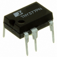
TNY377PN
Manufacturer Part Number
TNY377PN
Description
IC OFFLINE SWIT OVP OTP HV 8DIP
Manufacturer
Power Integrations
Series
TinySwitch®-PKr
Type
Off Line Switcherr
Datasheet
1.TNY376PN.pdf
(22 pages)
Specifications of TNY377PN
Output Isolation
Isolated
Frequency Range
132 ~ 280kHz
Voltage - Output
700V
Power (watts)
28W
Operating Temperature
-40°C ~ 150°C
Package / Case
8-DIP (0.300", 7.62mm), 7 Leads
Output Voltage
700 V
Input / Supply Voltage (max)
9 V
Input / Supply Voltage (min)
- 0.3 V
Duty Cycle (max)
65 %
Switching Frequency
264 KHz
Supply Current
570 uA
Operating Temperature Range
- 40 C to + 150 C
Mounting Style
Through Hole
Maximum Operating Temperature
+ 150 C
Minimum Operating Temperature
- 40 C
Output Current
1.4 A
Output Power
28 W
Lead Free Status / RoHS Status
Lead free / RoHS Compliant
Other names
596-1144-5
Available stocks
Company
Part Number
Manufacturer
Quantity
Price
Company:

Part Number:
TNY377PN
Manufacturer:
POWER
Quantity:
15 000


should be located as close as possible to the SOURCE and
BYPASS pins of the device.
For best performance of the OVP function, it is recommended
that a relatively high bias winding voltage is used, in the range
of 15 V-30 V. This minimizes the error voltage on the bias
winding due to leakage inductance and also ensures adequate
voltage during no-load operation from which to supply the IC
device consumption.
Selecting the Zener diode voltage to be approximately 6 V
above the bias winding voltage (28 V for 22 V bias winding)
gives good OVP performance for most designs but can be
adjusted to compensate for variations in leakage inductance.
Adding additional fi ltering can be achieved by inserting a low
value (10 Ω to 47 Ω) resistor in series with the bias winding
diode and/or the OVP Zener, as shown by R4 and R5 in
Figure 15. The resistor in series with the OVP Zener also limits
the maximum current into the BYPASS pin.
Reducing No-load Consumption
With the exception of the TNY375 and TNY376, a bias winding
must be used to provide supply current for the IC. This has the
additional benefi t of reducing the typical no-load consumption
to <60 mW. Select the value of the resistor (R6 in Figure 15) to
provide the data sheet supply current equal to I
in practice the bias voltage falls at low load, the reduction in
supply current through R6 is balanced against the reduced IC
consumption as the effective switching frequency reduces with
load.
Audible Noise
The cycle skipping mode of operation used in the TinySwitch-PK
devices can generate audio frequency components in the
transformer. To limit this audible noise generation, the
transformer should be designed such that the peak core fl ux
density is below 3000 Gauss (300 mT). Following this guideline,
and using the standard transformer production technique of dip
varnishing practically eliminates audible noise. Vacuum
impregnation of the transformer should not be used due to the
high primary capacitance and increased losses that results.
Ceramic capacitors that use dielectrics such as Z5U, when
used in clamp circuits, may also generate audio noise. If this is
the case, try replacing them with a capacitor having a different
dielectric or construction such as the fi lm foil or metallized foil type.
TinySwitch-PK Layout Considerations
Single Point Grounding
Use a single point ground connection from the input fi lter
capacitor to the area of copper connected to the SOURCE pins.
When used as an auxiliary supply in a larger converter, a local
DC bus decoupling capacitor is recommended. A value of
100 nF is typical.
The bias winding should be returned directly to the input or
decoupling capacitor. This routes surge currents away from the
device during common mode line surge events.
Rev. C 07/09
10
TNY375-380
S2
+ |I
DIS
|. Although
Bypass Capacitor (C
The BYPASS pin capacitor should be located as near as
possible to the BYPASS and SOURCE pins using a Kelvin
connection. No power current should fl ow through traces
connected to the BYPASS pin capacitor or optocoupler. If
using SMD components, a capacitor can be placed underneath
the package directly between BP and SOURCE pins.
When using a capacitor value of 1 μF or 10 μF to select the
reduced or increased current limit mode, it is recommended
that an additional 0.1 μF ceramic capacitor is placed directly
between BP and SOURCE pins.
Enable/Undervoltage Pin Node Connections
The EN/UV pin is a low-current, low-voltage pin, and noise
coupling can cause poor regulation and/or inaccurate line UV
levels. Traces connected to the EN/UV pin must be routed
away from any high current or high-voltage switching nodes,
including the drain pin and clamp components. This also
applies to the placement of the line undervoltage sense resistor
(R
this component.
TinySwitch-PK determines the presence of the UV resistor via a
~1 μA current into the EN/UV pin at startup. When the under-
voltage feature is not used ensure that leakage current into the
EN/UV pin is <<1 μA. This prevents false detection of the
presence of a UV resistor which may prevent correct start-up.
As the use of no-clean fl ux may increase leakage currents (by
reducing surface resistivity) care should be taken to follow the
fl ux suppliers guidance, specifi cally avoiding fl ux contamination.
Placing a 100 kΩ, 5% resistor between BP and EN/UV pins
eliminates this requirement by feeding current >I
EN/UV pin.
Primary Loop Area
The area of the primary loop that connects the input fi lter
capacitor, transformer primary, and TinySwitch-PK device
should be kept as small as possible.
Primary Clamp Circuit
A clamp is used to limit peak voltage on the DRAIN pin at turn
off. This can be achieved by using an RCD clamp or a Zener
and diode clamp across the primary winding. In all cases, to
minimize EMI, care should be taken to minimize the loop length
from the clamp components to the transformer and the
TinySwitch-PK device.
Thermal Considerations
The four SOURCE pins are internally connected to the IC lead
frame and provide the main path to remove heat from the
device. Therefore all the SOURCE pins should be connected to
a copper area underneath the TinySwitch-PK integrated circuit
to act not only as a single point ground, but also as a heatsink.
As this area is connected to the quiet source node, it should be
maximized for good heatsinking. Similarly, for axial output
diodes, maximize the PCB area connected to the cathode.
UV
). Drain connected traces must not be routed underneath
BP
)
www.powerint.com
LUV(MAX)
into the
Related parts for TNY377PN
Image
Part Number
Description
Manufacturer
Datasheet
Request
R

Part Number:
Description:
SOP-16
Manufacturer:
Power Integrations
Datasheet:
Part Number:
Description:
DIP8
Manufacturer:
Power Integrations
Datasheet:
Part Number:
Description:
TO-263
Manufacturer:
Power Integrations
Datasheet:
Part Number:
Description:
TO-263
Manufacturer:
Power Integrations
Datasheet:
Part Number:
Description:
Manufacturer:
Power Integrations
Datasheet: