TNY377PN Power Integrations, TNY377PN Datasheet - Page 2
TNY377PN
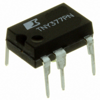
Manufacturer Part Number
TNY377PN
Description
IC OFFLINE SWIT OVP OTP HV 8DIP
Manufacturer
Power Integrations
Series
TinySwitch®-PKr
Type
Off Line Switcherr
Datasheet
1.TNY376PN.pdf
(22 pages)
Specifications of TNY377PN
Output Isolation
Isolated
Frequency Range
132 ~ 280kHz
Voltage - Output
700V
Power (watts)
28W
Operating Temperature
-40°C ~ 150°C
Package / Case
8-DIP (0.300", 7.62mm), 7 Leads
Output Voltage
700 V
Input / Supply Voltage (max)
9 V
Input / Supply Voltage (min)
- 0.3 V
Duty Cycle (max)
65 %
Switching Frequency
264 KHz
Supply Current
570 uA
Operating Temperature Range
- 40 C to + 150 C
Mounting Style
Through Hole
Maximum Operating Temperature
+ 150 C
Minimum Operating Temperature
- 40 C
Output Current
1.4 A
Output Power
28 W
Lead Free Status / RoHS Status
Lead free / RoHS Compliant
Other names
596-1144-5
Available stocks
Company
Part Number
Manufacturer
Quantity
Price
Company:

Part Number:
TNY377PN
Manufacturer:
POWER
Quantity:
15 000


Rev. C 07/09
Figure 2
Pin Functional Description
DRAIN (D) Pin:
This pin is the power MOSFET drain connection. It provides
internal operating current for both start-up and steady-state
operation.
BYPASS/MULTI-FUNCTION (BP/M) Pin:
This pin has multiple functions:
1.
2.
3.
MULTI-FUNCTION
2
It is the connection point for an external bypass capacitor for
the internally generated 5.85 V supply.
It is a mode selector for the current limit value, depending on
the value of the capacitance added. Use of a 0.1 μF
capacitor results in the standard current limit value. Use of a
1 μF capacitor results in the current limit being reduced to
that of the next smaller device size. Use of a 10 μF capacitor
results in the current limit being increased to that of the next
larger device.
It provides a shutdown function. When the current into the
bypass pin exceeds 7 mA, the device latches off until the
BP/M voltage drops below 4.9 V, during a power down or
when a line undervoltage is detected. This can be used to
provide an output overvoltage function with a Zener diode
connected from the BP/M pin to a bias winding supply.
VOLTAGE
ENABLE/
115 μA
UNDER-
BYPASS/
(EN/UV)
(BP/M)
Functional Block Diagram.
TNY375-380
ENABLE
1.0 V + V
1.0 V
25 μA
T
6.4 V
LINE UNDER-VOLTAGE
OSCILLATOR
JITTER 2X
LATCH
RESET
COUNTER
OVP
RESTART
DC MAX
CLOCK
AUTO-
RESET
PRESENT
FAULT
ENABLE/UNDERVOLTAGE (EN/UV) Pin:
This pin has dual functions: enable input and line undervoltage
sense. During normal operation, switching of the power
MOSFET is controlled by this pin. MOSFET switching is
terminated when a current greater than a threshold current is
drawn from this pin. Switching resumes when the current being
Figure 3.
SELECT AND
LIMIT STATE
CAPACITOR
CURRENT
MACHINE
BYPASS
SHUTDOWN
THERMAL
Pin Confi guration.
S
R
5.85 V
4.9 V
EN/UV
Q
Q
BP/M
G Package (SMD-8C)
P Package (DIP-8C)
D Package (SO-8C)
+
D
-
1
2
4
BYPASS PIN
UNDER-VOLTAGE
REGULATOR
5.85 V
CURRENT LIMIT
COMPARATOR
BLANKING
LEADING
EDGE
8
7
6
5
V
I LIMIT
S
S
S
S
www.powerint.com
+
-
PI-4348-042809
PI-4550-121406
SOURCE
DRAIN
(D)
(S)
Related parts for TNY377PN
Image
Part Number
Description
Manufacturer
Datasheet
Request
R

Part Number:
Description:
SOP-16
Manufacturer:
Power Integrations
Datasheet:
Part Number:
Description:
DIP8
Manufacturer:
Power Integrations
Datasheet:
Part Number:
Description:
TO-263
Manufacturer:
Power Integrations
Datasheet:
Part Number:
Description:
TO-263
Manufacturer:
Power Integrations
Datasheet:
Part Number:
Description:
Manufacturer:
Power Integrations
Datasheet: