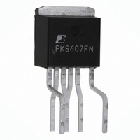
PKS607FN Power Integrations, PKS607FN Datasheet - Page 8

PKS607FN
Manufacturer Part Number
PKS607FN
Description
IC OFFLINE SWIT OTP OCP HV TO262
Manufacturer
Power Integrations
Series
PeakSwitch®r
Datasheet
1.PKS606PN.pdf
(24 pages)
Specifications of PKS607FN
Output Isolation
Isolated
Frequency Range
250 ~ 304kHz
Voltage - Output
700V
Power (watts)
126W
Operating Temperature
-40°C ~ 150°C
Package / Case
TO-262-7 (Formed Leads), 5 Leads
Input / Supply Voltage (max)
265 VAC
Input / Supply Voltage (min)
85 VAC
Duty Cycle (max)
68 %
Switching Frequency
277 kHz
Supply Current
1430 uA
Operating Temperature Range
- 40 C to + 150 C
Mounting Style
Through Hole
For Use With
596-1267 - KIT REF DESIGN PEAKSWITCH
Lead Free Status / RoHS Status
Lead free / RoHS Compliant
Other names
596-1140-5
Available stocks
Company
Part Number
Manufacturer
Quantity
Price
Company:
Part Number:
PKS607FN
Manufacturer:
POWER
Quantity:
15 000
Part Number:
PKS607FN
Manufacturer:
POWER
Quantity:
20 000
Figure 15. PeakSwitch PKS606Y, 32 W Continuous, 81 W Peak, Universal Input Power Supply.
Application Example
The circuit shown in Figure15 is a low cost, high efficiency,
flyback power supply designed to provide a 30 V, 1.06 A
continuous, 2.7 A peak output from universal input using the
PKS606Y.
The s upply f eatures u nder-voltage l ockout a nd s mart A C s ense w ith
fast reset. Latching overload, open loop, and hysteretic thermal
shutdown protect both the supply and load under fault conditions
while high efficiency (>80%) and very low no-load consumption
(<200 mW at 230 VAC) meets both active and standby efficiency
requirements. Output regulation is accomplished using a simple
Zener reference and opto coupler feedback.
Components C1, C2, C3, C10, C17, C19, R15, L1 and L2 provide
common mode and differential mode EMI filtering. Resistors
R1 and R2 discharge C3 when AC power is removed to prevent
electric shock from touching the AC input. Thermistor RT1
limits the peak inrush current when AC is first applied.
The rectified and filtered input voltage is applied to the primary
winding of T1. The other side of the transformer primary is
driven by the integrated MOSFET in U1. Diode D6, C5, R3,
R4, and VR1 clamp the U1 drain voltage to safe levels. Use
of a fast diode (500 ns) vs ultrafast for D6 increases power
supply efficiency by recovering some of the clamp energy. A
slow or standard recovery diode must not be used due to the
Rev. I 02/07
8
PE
J1
L
N
3.15 A
F1
1.3 MΩ
R2
PKS603-607
250 VAC
100 pF
680 nF
C1-C2
C3
X1
1.3 MΩ
R1
5.3 mH
L1
1N4007
D1-D4
t
10 Ω
O
RT1
1N4007
D5
150 µF
400 V
100 nF
C4
400 V
C7
4.7 nF
1 kV
C17
PeakSwitch
2.2 Ω
R15
PKS606Y
2.2 MΩ
U1
R5
RTN Connected to PE via Flying Lead
2.2 nF
1 kV
C5
1/2 W
22 Ω
FR106
R4
D6
2.4 MΩ
1N4764A
R6
100 V
VR1
10 kΩ
1/2 W
R3
2.7 MΩ
R16
1
3
2
250 VAC
1 nF
EE25
C10
T1
9,10
220 nF
7,8
4
5
high switching frequency (a slow diode will not recover fast
enough under startup or output faults and therefore fail due
to excess dissipation). The use of a Zener in series with R3
compared to a standard RCD clamp optimizes both EMI and
energy efficiency.
Components D5, C7, and R5-6 provide AC line and under-
voltage sensing for PeakSwitch U1. By providing a separate
rectified voltage across C7 which is independent from the load
condition, rather than using the main input capacitor, allows
PeakSwitch to distinguish the cause of loss of regulation. It
also provides fast reset when the AC input is removed, should
latching shutdown be triggered. Connecting R5 and R6 to C4
would still provide under-voltage lockout but after a fault the
user would have to wait for C4 to discharge before the supply
would reset. Resistor R16 provides a small amount of bias to
the U1 ENABLE/UNDER-VOLTAGE pin to retain the under-
voltage lockout function during brown-out conditions.
With R5 and R6 present, switching is inhibited until the current
into the EN/UV pin exceeds 25 µA. This allows the startup
voltage to be programmed within the normal operating input
voltage range, preventing glitching of the output under abnormal,
low voltage conditions and also on removal of the AC input.
Under a fault condition, for example an output short circuit or
broken feedback loop, if the line voltage is within the normal
range (>25 µA into the EN/UV pin) the PeakSwitch will latch
50 V
1N4148
C8
D7
47 µF
35 V
C6
STPS3150
1/2 W
68 Ω
R8
D8
PC817X4
1 nF, 250 VAC
U2
330 pF
C11
C19
4.7 kΩ
330 µF
R7
50 V
C12
1 kΩ
R12
1N4148
D9
1N5255B
VR2
28 V
2N3906
100 nF
50 V
1 kΩ
C15
R13
Q1
FS202DA
3 kΩ
R11
100 nF
UF4003
47 µF
C16
16 V
C13
Q2
D10
1.5 kΩ
0.33 Ω
R10
2 W
R9
PCB Term 18 AWG
5.3 µH
1N5258B
L2
100 Ω
36 V
VR3
R14
J3
PI-4170-060706
220 nF
50 V
C14
1.07 A Cont.
2.7 A Peak
30 V @
RTN


