PKS607FN Power Integrations, PKS607FN Datasheet - Page 12
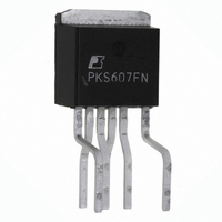
PKS607FN
Manufacturer Part Number
PKS607FN
Description
IC OFFLINE SWIT OTP OCP HV TO262
Manufacturer
Power Integrations
Series
PeakSwitch®r
Datasheet
1.PKS606PN.pdf
(24 pages)
Specifications of PKS607FN
Output Isolation
Isolated
Frequency Range
250 ~ 304kHz
Voltage - Output
700V
Power (watts)
126W
Operating Temperature
-40°C ~ 150°C
Package / Case
TO-262-7 (Formed Leads), 5 Leads
Input / Supply Voltage (max)
265 VAC
Input / Supply Voltage (min)
85 VAC
Duty Cycle (max)
68 %
Switching Frequency
277 kHz
Supply Current
1430 uA
Operating Temperature Range
- 40 C to + 150 C
Mounting Style
Through Hole
For Use With
596-1267 - KIT REF DESIGN PEAKSWITCH
Lead Free Status / RoHS Status
Lead free / RoHS Compliant
Other names
596-1140-5
Available stocks
Company
Part Number
Manufacturer
Quantity
Price
Company:

Part Number:
PKS607FN
Manufacturer:
POWER
Quantity:
15 000
Part Number:
PKS607FN
Manufacturer:
POWER
Quantity:
20 000


Thermal Considerations
For the P package, the four SOURCE pins are internally
connected to the IC lead frame and provide the main path to
remove heat from the device. Therefore, all the SOURCE pins
should be connected to a copper area underneath the PeakSwitch
to act not only as a single point ground, but also as a heatsink.
As this area is connected to the quiet source node, it should be
maximized for good heatsinking. Similarly, for axial output
diodes, maximize the PCB area connected to the cathode.
Y-Capacitor
The placement of the Y-type cap should be directly from the
primary input filter capacitor positive terminal to the common/
return terminal of the transformer secondary. If a second
Y- type cap is required from primary to secondary return, connect
the primary side directly to the negative terminal of the input
capacitor. Such a placement will route high magnitude common
mode surge currents away from the PeakSwitch device. Note
– if an input π (C, L, C) EMI filter is used, then the inductor in
the filter should be placed between the negative terminals on
the input filter capacitors.
Optocoupler
Place the optocoupler physically close to the PeakSwitch to
minimize the primary side trace lengths. Keep the high current
high voltage drain and clamp traces away from the optocoupler
to prevent noise pick up.
Output Diode
For best performance, the area of the loop connecting the
secondary winding, the output diode and the output filter
capacitor should be minimized. In addition, sufficient copper
area should be provided at the anode and cathode terminal
of the diode for heatsinking. A larger area is preferred at the
quite cathode terminal. A large anode area can increase high
frequency radiated EMI.
Rev. I 02/07
12
PKS603-607
Quick Design Checklist
As with any power supply design, all PeakSwitch designs
should be verified on the bench to make sure that component
specifications are not exceeded under worst case conditions. The
following minimum set of tests is strongly recommended:
1. Maximum drain voltage – Verify that the V
2. Maximum drain currents – Verify the simultaneous drain
3. Maximum drain current – A t maximum ambient temperature,
4. Thermal Check – At specified maximum output power,
Design Tools
Up-to-date information on design tools can be found at the
Power Integrations web site: www.powerint.com.
650 V at highest input voltage and peak (overload) output
power. The 50 V margin to the 700 V BV
allows margin for design variation.
voltage and current levels are within the curve provided in
Figure 29 under worst case conditions. Typically this occurs
at start up (and during an output short circuit), highest input
line voltage and maximum ambient temperature. When
making this measurement using a current probe, to monitor
the drain current, ensure the results are corrected for the
10-20 ns current probe delay.
maximum input voltage and peak output (overload) power,
verify drain current waveforms show no signs of transformer
saturation. If the transformer shows signs of saturation,
it should be redesigned with a lower flux density, or a
higher quality core material should be used. To prevent
false triggering of the current limit, verify the leading
edge current spike event is below I
t
should be below the absolute maximum limit specified in
the Absolute Maximum Ratings section.
minimum input voltage and maximum ambient temperature,
verify that the temperature specifications are not exceeded for
PeakSwitch, transformer, output diode and output capacitors.
Enough thermal margin should be allowed for part-to-part
variation of the R
data sheet. Under low line, maximum power, a maximum
PeakSwitch SOURCE pin or tab temperature of 110 °C is
recommended to allow for these variations.
LEB(MIN)
. Under all conditions, the maximum drain current
DS(ON)
of PeakSwitch as specified in the
INIT(MIN)
DS
at the end of the
DSS
does not exceed
specification
Related parts for PKS607FN
Image
Part Number
Description
Manufacturer
Datasheet
Request
R

Part Number:
Description:
SOP-16
Manufacturer:
Power Integrations
Datasheet:
Part Number:
Description:
DIP8
Manufacturer:
Power Integrations
Datasheet:
Part Number:
Description:
TO-263
Manufacturer:
Power Integrations
Datasheet:
Part Number:
Description:
TO-263
Manufacturer:
Power Integrations
Datasheet:
Part Number:
Description:
Manufacturer:
Power Integrations
Datasheet: