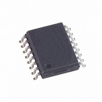
EPCS16SI16N Altera, EPCS16SI16N Datasheet - Page 21

EPCS16SI16N
Manufacturer Part Number
EPCS16SI16N
Description
IC CONFIG DEVICE 16MBIT 16-SOIC
Manufacturer
Altera
Series
EPCSr
Specifications of EPCS16SI16N
Programmable Type
In System Programmable
Memory Size
16Mb
Voltage - Supply
3 V ~ 3.6 V
Operating Temperature
-40°C ~ 85°C
Package / Case
16-SOIC (0.300", 7.50mm Width)
Memory Type
Flash
Clock Frequency
20MHz
Supply Voltage Range
2.7V To 3.6V
Memory Case Style
SOIC
No. Of Pins
16
Operating Temperature Range
-40°C To +85°C
Rohs Compliant
Yes
Lead Free Status / RoHS Status
Lead free / RoHS Compliant
Other names
544-1240-5
EPCS16SI16
EPCS16SI16
Available stocks
Company
Part Number
Manufacturer
Quantity
Price
Company:
Part Number:
EPCS16SI16N
Manufacturer:
ALTERA
Quantity:
1 250
Company:
Part Number:
EPCS16SI16N
Manufacturer:
ALTERA44
Quantity:
540
Part Number:
EPCS16SI16N
Manufacturer:
ALTERA/阿尔特拉
Quantity:
20 000
Chapter 3: Serial Configuration Devices (EPCS1, EPCS4, EPCS16, EPCS64, and EPCS128) Data Sheet
Serial Configuration Device Memory Access
Figure 3–11. Read Bytes Operation Timing Diagram
Notes to
(1) Address bit A[23] is a don't-care bit in EPCS64. Address bits A[23..21] are don't-care bits in EPCS16. Address bits A[23..19] are don't-care
(2) For .rpd files, the read sequence shifts out the LSB of the data byte first.
June 2011 Altera Corporation
bits in EPCS4. Address bits A[23..17] are don't-care bits in the EPCS1.
Figure
DCLK
DATA
ASDI
nCS
3–11:
Read Bytes Operation
The read bytes operation code is b'0000 0011, with the MSB listed first. To read the
memory contents of the serial configuration device, the device is first selected by
driving nCS low. Then, the read bytes operation code is shifted in followed by a 3-byte
address (A[23..0]). Each address bit must be latched in on the rising edge of the DCLK.
After the address is latched in, the memory contents of the specified address are
shifted out serially on the DATA pin, beginning with the MSB. For reading Raw
Programming Data files (.rpd), the content is shifted out serially beginning with the
LSB. Each data bit is shifted out on the falling edge of DCLK. The maximum DCLK
frequency during the read bytes operation is 20 MHz.
diagram for the read bytes operation.
The first byte address can be at any location. The device automatically increments the
address to the next higher address after shifting out each byte of data. Therefore, the
device can read the whole memory with a single read bytes operation. When the
device reaches the highest address, the address counter restarts at 0x000000, allowing
the memory contents to be read out indefinitely until the read bytes operation is
terminated by driving nCS high. The device can drive nCS high any time after data is
shifted out. If the read bytes operation is shifted in while a write or erase cycle is in
progress, the operation is not executed and has no effect on the write or erase cycle in
progress.
Fast Read Operation
The device is first selected by driving nCS low. The fast read instruction code is
followed by a 3-byte address (A23-A0) and a dummy byte, each bit being latched-in
during the rising edge of DCLK. Then the memory contents, at that address, is shifted
out on DATA, each bit being shifted out, at a maximum frequency of 40 MHz, during
the falling edge of DCLK.
The instruction sequence is shown in
The first byte addressed can be at any location. The address is automatically
incremented to the next higher address after each byte of data is shifted out. The
whole memory can, therefore, be read with a single fast read instruction. When the
highest address is reached, the address counter rolls over to 000000h, allowing the
read sequence to be continued indefinitely.
0
High Impedance
1
2
Operation Code
3
4
5
6
7
MSB
23
8
22
9
21
10
24-Bit Address (1)
Figure
3
28
2
29
1
30
3–12.
0
31
MSB (2)
7
32
6
33
Figure 3–11
5
34
DATA Out 1
4
35
Volume 2: Configuration Handbook
3
36
2
37
shows the timing
1
38
0
39
DATA Out 2
7
3–21


