EPCS16SI16N Altera, EPCS16SI16N Datasheet - Page 16
EPCS16SI16N
Manufacturer Part Number
EPCS16SI16N
Description
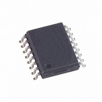
IC CONFIG DEVICE 16MBIT 16-SOIC
Manufacturer
Altera
Series
EPCSr
Specifications of EPCS16SI16N
Programmable Type
In System Programmable
Memory Size
16Mb
Voltage - Supply
3 V ~ 3.6 V
Operating Temperature
-40°C ~ 85°C
Package / Case
16-SOIC (0.300", 7.50mm Width)
Memory Type
Flash
Clock Frequency
20MHz
Supply Voltage Range
2.7V To 3.6V
Memory Case Style
SOIC
No. Of Pins
16
Operating Temperature Range
-40°C To +85°C
Rohs Compliant
Yes
Lead Free Status / RoHS Status
Lead free / RoHS Compliant
Other names
544-1240-5
EPCS16SI16
EPCS16SI16
Available stocks
Company
Part Number
Manufacturer
Quantity
Price
Company:

Part Number:
EPCS16SI16N
Manufacturer:
ALTERA
Quantity:
1 250
Company:
Part Number:
EPCS16SI16N
Manufacturer:
ALTERA44
Quantity:
540
Part Number:
EPCS16SI16N
Manufacturer:
ALTERA/阿尔特拉
Quantity:
20 000


3–16
Table 3–8. Operation Codes for Serial Configuration Devices
Volume 2: Configuration Handbook
Write enable
Write disable
Read status
Read bytes
Read silicon ID
Fast read
Write status
Write bytes
Erase bulk
Erase sector
Read Device
Identification
Notes to
(1) The MSB is listed first and the least significant bit (LSB) is listed last.
(2) The status register, data or silicon ID are read out at least once on the DATA pin and will continuously be read out until nCS is driven high.
(3) Write bytes operation requires at least one data byte on the DATA pin. If more than 256 bytes are sent to the device, only the last 256 bytes are
(4) Read silicon ID operation is available only for EPCS1, EPCS4, EPCS16, and EPCS64.
(5) Read Device Identification operation is available only for EPCS128.
written to the memory.
Operation
Table
3–8:
(5)
(4)
For the write byte, erase bulk, erase sector, write enable, write disable, and write
status operations, drive the nCS pin high exactly at a byte boundary (drive the nCS pin
high a multiple of eight clock pulses after the nCS pin is driven low); otherwise, the
operation is rejected and is not executed.
All attempts to access the memory contents while a write or erase cycle is in progress
will not be granted, and the write or erase cycle will continue unaffected.
Write Enable Operation
The write enable operation code is b'0000 0110, and the MSB is listed first. The write
enable operation sets the write enable latch bit, which is bit 1 in the status register.
Always set the write enable latch bit before write bytes, write status, erase bulk, and
erase sector operations.
operation.
Figure 3–5. Write Enable Operation Timing Diagram
Operation Code
0000 0110
0000 0100
0000 0101
0000 0011
1010 1011
0000 1011
0000 0001
0000 0010
1100 0111
1101 1000
1001 1111
Figure 3–7
Chapter 3: Serial Configuration Devices (EPCS1, EPCS4, EPCS16, EPCS64, and EPCS128) Data Sheet
(1)
DCLK
DATA
ASDI
nCS
and
Address Bytes
Figure 3–5
Figure 3–8
0
0
0
3
0
3
0
3
0
3
0
High Impedance
shows the timing diagram for the write enable
0
show the status register bit definitions.
1
Dummy Bytes
2
Operation Code
3
0
0
0
0
3
1
0
0
0
0
2
4
5
6
Serial Configuration Device Memory Access
7
1 to infinite
1 to infinite
1 to infinite
1 to infinite
1 to infinite
1 to 256
Data Bytes
0
0
1
0
0
June 2011 Altera Corporation
(3)
(2)
(2)
(2)
(2)
(2)
DCLK f
(MHz)
25
25
25
20
25
40
25
25
25
25
25
MAX
Related parts for EPCS16SI16N
Image
Part Number
Description
Manufacturer
Datasheet
Request
R

Part Number:
Description:
IC CONFIG DEVICE 1MBIT 8-SOIC
Manufacturer:
Altera
Datasheet:
Part Number:
Description:
IC CONFIG DEVICE 4MBIT 8-SOIC
Manufacturer:
Altera
Datasheet:
Part Number:
Description:
IC CONFIG DEVICE 4MBIT 8-SOIC
Manufacturer:
Altera
Datasheet:
Part Number:
Description:
IC CONFIG DEVICE 16MBIT 8-SOIC
Manufacturer:
Altera
Datasheet:

Part Number:
Description:
IC CONFIG DEVICE 64MBIT 16-SOIC
Manufacturer:
Altera
Datasheet:
Part Number:
Description:
IC CONFIG DEVICE 1MBIT 8-SOIC
Manufacturer:
Altera
Datasheet:

Part Number:
Description:
CYCLONE II STARTER KIT EP2C20N
Manufacturer:
Altera
Datasheet:


Part Number:
Description:
CPLD, EP610 Family, ECMOS Process, 300 Gates, 16 Macro Cells, 16 Reg., 16 User I/Os, 5V Supply, 35 Speed Grade, 24DIP
Manufacturer:
Altera Corporation
Datasheet:
Part Number:
Description:
CPLD, EP610 Family, ECMOS Process, 300 Gates, 16 Macro Cells, 16 Reg., 16 User I/Os, 5V Supply, 15 Speed Grade, 24DIP
Manufacturer:
Altera Corporation
Datasheet:
Part Number:
Description:
Manufacturer:
Altera Corporation
Datasheet:
Part Number:
Description:
CPLD, EP610 Family, ECMOS Process, 300 Gates, 16 Macro Cells, 16 Reg., 16 User I/Os, 5V Supply, 30 Speed Grade, 24DIP
Manufacturer:
Altera Corporation
Datasheet:
Part Number:
Description:
High-performance, low-power erasable programmable logic devices with 8 macrocells, 10ns
Manufacturer:
Altera Corporation
Datasheet: