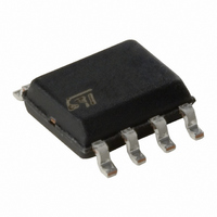
M95010-WMN6P STMicroelectronics, M95010-WMN6P Datasheet - Page 17

M95010-WMN6P
Manufacturer Part Number
M95010-WMN6P
Description
IC EEPROM 1KBIT 10MHZ 8SOIC
Manufacturer
STMicroelectronics
Specifications of M95010-WMN6P
Format - Memory
EEPROMs - Serial
Memory Type
EEPROM
Memory Size
1K (128 x 8)
Speed
10MHz
Interface
SPI, 3-Wire Serial
Voltage - Supply
2.5 V ~ 5.5 V
Operating Temperature
-40°C ~ 85°C
Package / Case
8-SOIC (3.9mm Width)
Memory Configuration
128 X 8
Interface Type
Serial, SPI
Clock Frequency
10MHz
Supply Voltage Range
2.5V To 5.5V
Memory Case Style
SO
No. Of Pins
8
Rohs Compliant
Yes
Lead Free Status / RoHS Status
Lead free / RoHS Compliant
Other names
497-8600-5
M95010-WMN6P
M95010-WMN6P
Available stocks
Company
Part Number
Manufacturer
Quantity
Price
Write to Memory Array (WRITE)
As shown in
the device, Chip Select (S) is first driven Low. The
bits of the instruction byte, address byte, and at
least one data byte are then shifted in, on Serial
Data Input (D).
The instruction is terminated by driving Chip Se-
lect (S) High after the rising edge of Serial Clock
(C) that latches the last data bit, and before the
next rising edge of Serial Clock (C) occurs any-
where on the bus. In the case of
occurs after the eighth bit of the data byte has
been latched in, indicating that the instruction is
being used to write a single byte. The self-timed
Write cycle starts, and continues for a period t
(as specified in
of which the Write in Progress (WIP) bit is reset to
0.
If, though, Chip Select (S) continues to be driven
Low, as shown in
data is shifted in. In this way, all the bytes from the
Figure 13. Byte Write (WRITE) Sequence
Note: Depending on the memory size, as shown in
S
C
D
Q
Figure
Table 18.
Figure
13., to send this instruction to
0
1
High Impedance
14., the next byte of input
to
2
Instruction
Table
3
A8
4
Figure
22.), at the end
5
6
Table
7
13., this
A7
8
6., the most significant address bits are Don’t Care.
A6 A5 A4 A3 A2 A1 A0
9 10 11 12 13 14 15 16 17 18 19
WC
Byte Address
given address to the end of the same page can be
programmed in a single instruction.
If Chip Select (S) still continues to be driven Low,
the next byte of input data is shifted in, and is used
to overwrite the byte at the start of the current
page.
The instruction is not accepted, and is not execut-
ed, under the following conditions:
–
–
–
–
if the Write Enable Latch (WEL) bit has not
been set to 1 (by executing a Write Enable
instruction just before)
if a Write cycle is already in progress
if the device has not been deselected, by Chip
Select (S) being driven High, at a byte
boundary (after the rising edge of Serial Clock
(C) that latches the last data bit, and before
the next rising edge of Serial Clock (C) occurs
anywhere on the bus)
if Write Protect (W) is Low or if the addressed
page is in the region protected by the Block
Protect (BP1 and BP0) bits.
7
6
5
Data Byte
M95040, M95020, M95010
4
3
20 21 22 23
2
1
0
AI01442D
17/37


