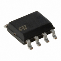
M95010-WMN6P STMicroelectronics, M95010-WMN6P Datasheet - Page 10

M95010-WMN6P
Manufacturer Part Number
M95010-WMN6P
Description
IC EEPROM 1KBIT 10MHZ 8SOIC
Manufacturer
STMicroelectronics
Specifications of M95010-WMN6P
Format - Memory
EEPROMs - Serial
Memory Type
EEPROM
Memory Size
1K (128 x 8)
Speed
10MHz
Interface
SPI, 3-Wire Serial
Voltage - Supply
2.5 V ~ 5.5 V
Operating Temperature
-40°C ~ 85°C
Package / Case
8-SOIC (3.9mm Width)
Memory Configuration
128 X 8
Interface Type
Serial, SPI
Clock Frequency
10MHz
Supply Voltage Range
2.5V To 5.5V
Memory Case Style
SO
No. Of Pins
8
Rohs Compliant
Yes
Lead Free Status / RoHS Status
Lead free / RoHS Compliant
Other names
497-8600-5
M95010-WMN6P
M95010-WMN6P
Available stocks
Company
Part Number
Manufacturer
Quantity
Price
M95040, M95020, M95010
Status Register
Figure 7.
in the control logic of the device. This register con-
tains a number of control bits and status bits, as
shown in
Bits b7, b6, b5 and b4 are always read as 1.
WIP bit. The Write In Progress bit is a volatile
read-only bit that is automatically set and reset by
the internal logic of the device. When set to a 1, it
indicates that the memory is busy with a Write cy-
cle.
WEL bit. The Write Enable Latch bit is a volatile
read-only bit that is set and reset by specific in-
structions. When reset to 0, no WRITE or WRSR
instructions are accepted by the device.
BP1, BP0 bits. The Block Protect bits are non-
volatile read-write bits. These bits define the area
of memory that is protected against the execution
of Write cycles, as summarized in
Table 3. Status Register Format
Table 4. Write-Protected Block Size
10/37
b7
1
Status Register Bits
BP1
0
0
1
1
1
shows the position of the Status Register
Table
1
3..
BP0
0
1
0
1
Block Protect Bits
Write Enable Latch Bit
1
BP1
Protected Block
Whole memory
Write In Progress Bit
Upper quarter
Upper half
BP0
none
Table
WEL
4..
WIP
b0
180h - 1FFh
100h - 1FFh
000h - 1FFh
M95040
none
Data Protection and Protocol Control
To help protect the device from data corruption in
noisy or poorly controlled environments, a number
of safety features have been built in to the device.
The main security measures can be summarized
as follows:
–
–
–
–
For any instruction to be accepted and executed,
Chip Select (S) must be driven High after the rising
edge of Serial Clock (C) that latches the last bit of
the instruction, and before the next rising edge of
Serial Clock (C).
For this, “the last bit of the instruction” can be the
eighth bit of the instruction code, or the eighth bit
of a data byte, depending on the instruction (ex-
cept in the case of RDSR and READ instructions).
Moreover, the "next rising edge of CLOCK" might
(or might not) be the next bus transaction for some
other device on the bus.
When a Write cycle is in progress, the device pro-
tects it against external interruption by ignoring
any subsequent READ, WRITE or WRSR instruc-
tion until the present cycle is complete.
The WEL bit is reset at power-up.
Chip Select (S) must rise after the eighth clock
count (or multiple thereof) in order to start a
non-volatile Write cycle (in the memory array
or in the Status Register).
Accesses to the memory array are ignored
during the non-volatile programming cycle,
and the programming cycle continues
unaffected.
Invalid Chip Select (S) and Hold (HOLD)
transitions are ignored.
Array Addresses Protected
C0h - FFh
80h - FFh
00h - FFh
M95020
none
60h - 7Fh
40h - 7Fh
00h - 7Fh
M95010
none


