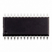
M48Z35AV-10MH6E STMicroelectronics, M48Z35AV-10MH6E Datasheet - Page 7

M48Z35AV-10MH6E
Manufacturer Part Number
M48Z35AV-10MH6E
Description
IC NVSRAM 256KBIT 100NS 28SOIC
Manufacturer
STMicroelectronics
Type
NVSRAMr
Specifications of M48Z35AV-10MH6E
Format - Memory
RAM
Memory Type
NVSRAM (Non-Volatile SRAM)
Memory Size
256K (32K x 8)
Speed
100ns
Interface
Parallel
Voltage - Supply
3 V ~ 3.6 V
Operating Temperature
-40°C ~ 85°C
Package / Case
28-SOIC, 28-SOH (8.48mm Width)
Word Size
8b
Organization
32Kx8
Density
256Kb
Interface Type
Parallel
Access Time (max)
100ns
Operating Supply Voltage (typ)
3.3V
Package Type
SOH
Operating Temperature Classification
Industrial
Operating Supply Voltage (max)
3.6V
Operating Supply Voltage (min)
3V
Operating Temp Range
-40C to 85C
Pin Count
28
Mounting
Surface Mount
Supply Current
50mA
Lead Free Status / RoHS Status
Contains lead / RoHS non-compliant
Other names
497-2881-5
M48Z35AV-10MH6
M48Z35AV-10MH6
Available stocks
Company
Part Number
Manufacturer
Quantity
Price
Table 3. READ Mode AC Characteristics
Note: 1. Valid for Ambient Operating Temperature: T
WRITE Mode
The M48Z35AY/V is in the WRITE Mode whenev-
er W and E are low. The start of a WRITE is refer-
enced from the latter occurring falling edge of W or
E. A WRITE is terminated by the earlier rising
edge of W or E. The addresses must be held valid
throughout the cycle. E or W must return high for
a minimum of t
from WRITE Enable prior to the initiation of anoth-
Figure 8. WRITE Enable Controlled, WRITE Mode AC Waveforms
Symbol
t
t
t
t
GLQX
EHQZ
GHQZ
ELQX
t
t
t
t
t
GLQV
AXQX
AVQV
ELQV
AVAV
2. C
(2)
(2)
(2)
(2)
L
= 5pF (see
A0-A14
E
W
DQ0-DQ7
READ Cycle Time
Address Valid to Output Valid
Chip Enable Low to Output Valid
Output Enable Low to Output Valid
Chip Enable Low to Output Transition
Output Enable Low to Output Transition
Chip Enable High to Output Hi-Z
Output Enable High to Output Hi-Z
Address Transition to Output Transition
EHAX
Figure 12., page
from Chip Enable or t
Parameter
12).
tAVEL
tAVWL
(1)
A
tWLQZ
= 0 to 70°C or –40 to 85°C; V
WHAX
tAVWH
tWLWH
tAVAV
VALID
er READ or WRITE cycle. Data-in must be valid t
VWH
t
WRITE cycles to avoid bus contention; although, if
the output bus has been activated by a low on E
and G, a low on W will disable the outputs t
after W falls.
Min
WHDX
70
10
5
5
M48Z35AY
prior to the end of WRITE and remain valid for
–70
tDVWH
afterward. G should be kept high during
CC
DATA INPUT
Max
= 4.5 to 5.5V or 3.0 to 3.6V (except where noted).
tWHDX
70
70
35
25
25
Min
100
M48Z35AY, M48Z35AV
10
10
5
M48Z35AV
tWHQX
–100
tWHAX
Max
100
100
50
50
40
AI00926
Unit
ns
ns
ns
ns
ns
ns
ns
ns
ns
WLQZ
7/21
D-


