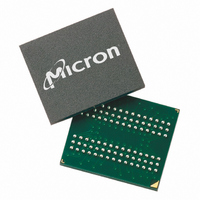
MT48H16M32LFCM-75 IT:A TR Micron Technology Inc, MT48H16M32LFCM-75 IT:A TR Datasheet - Page 51

MT48H16M32LFCM-75 IT:A TR
Manufacturer Part Number
MT48H16M32LFCM-75 IT:A TR
Description
IC SDRAM 512MBIT 133MHZ 90VFBGA
Manufacturer
Micron Technology Inc
Type
Mobile SDRAMr
Specifications of MT48H16M32LFCM-75 IT:A TR
Format - Memory
RAM
Memory Type
Mobile SDRAM
Memory Size
512M (16M x 32)
Speed
133MHz
Interface
Parallel
Voltage - Supply
1.7 V ~ 1.95 V
Operating Temperature
-40°C ~ 85°C
Package / Case
90-VFBGA
Organization
16Mx32
Density
512Mb
Address Bus
15b
Access Time (max)
8/5.4ns
Maximum Clock Rate
133MHz
Operating Supply Voltage (typ)
1.8V
Package Type
VFBGA
Operating Temp Range
-40C to 85C
Operating Supply Voltage (max)
1.95V
Operating Supply Voltage (min)
1.7V
Supply Current
95mA
Pin Count
90
Mounting
Surface Mount
Operating Temperature Classification
Industrial
Lead Free Status / RoHS Status
Lead free / RoHS Compliant
Other names
557-1329-2
Table 16:
Table 17:
Notes
PDF: 09005aef81ca5de4/Source: 09005aef81ca5e03
MT48H32M16LF_1.fm - Rev. J 2/08 EN
Parameter
Parameter
Input capacitance: CLK
Input capacitance: All other input-only balls
Input/Output capacitance: DQs
Input capacitance: CLK
Input capacitance: All other input-only balls
Input/Output capacitance: DQs
Capacitance (x16)
Note: 2; notes appear on pages 51–52
Capacitance (x32)
Note: 2; notes appear on pages 51–52
10.
11. AC timing and I
1. All voltages referenced to V
2. This parameter is sampled. V
3.
4. Enables on-chip refresh and address counters.
5. The minimum specifications are used only to indicate cycle time at which proper
6. An initial pause of 100µs is required after power-up, followed by two AUTO REFRESH
7. AC characteristics assume
8. In addition to meeting the transition rate specification, the clock and CKE must tran-
9. Outputs measured for 1.8V at 0.9V with equivalent load:
0.9V, 1.25V, and 1.4V, respectively; f = 1 MHz.
I
with minimum cycle time and the outputs open.
operation over the full temperature range (–40°C ≤ T
ensured.
commands, before proper device operation is ensured. (V
ered up simultaneously. V
REFRESH command wake-ups should be repeated any time the
ment is exceeded.
sit between V
Test loads with full DQ driver strength. Performance will vary with actual system DQ
bus capacitive loading, termination, and programmed drive strength.
t
a reference to V
High-Z.
point. If the input transition time is longer than
enced at V
Q
DD
HZ defines the time at which the output achieves the open circuit condition; it is not
is dependent on output loading and cycle rates. Specified values are obtained
IL
(MAX) and V
IH
20pF
OH
and V
DD
or V
tests have V
512Mb: 32 Meg x 16, 16 Meg x 32 Mobile SDRAM
IL
OL
(or between V
. The last valid data element will meet
IH
SS
t
51
SS
T = 1ns.
(MIN) and no longer at the V
and V
.
DD
IL
, V
and V
SS
DD
Symbol
Symbol
Q must be at same potential.) The two AUTO
Micron Technology, Inc., reserves the right to change products or specifications without notice.
Q = +1.8V; T
C
C
C
C
C
C
IL
IO
IO
I1
I2
I1
I2
IH
and V
, with timing referenced to V
IH
) in a monotonic manner.
t
T (MAX), then the timing is refer-
A
Min
Min
= 25°C; ball under test biased at
2.0
2.0
2.5
2.0
2.0
2.5
A
≤ +85°C for T
IH
DD
/2 crossover point.
©2005 Micron Technology, Inc. All rights reserved.
and V
t
Max
Max
OH before going
5.0
5.0
6.0
5.0
5.0
6.0
t
REF refresh require-
A
DD
on IT parts) is
IH
Q must be pow-
/2 = crossover
Units
Units
pF
pF
pF
pF
pF
pF
Notes


