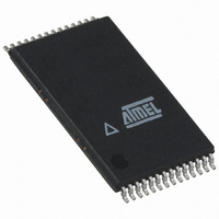
AT45DB321C-TC Atmel, AT45DB321C-TC Datasheet - Page 6

AT45DB321C-TC
Manufacturer Part Number
AT45DB321C-TC
Description
IC FLASH 32MBIT 40MHZ 28TSOP
Manufacturer
Atmel
Datasheet
1.AT45DB321C-RU.pdf
(40 pages)
Specifications of AT45DB321C-TC
Format - Memory
FLASH
Memory Type
DataFLASH
Memory Size
32M (8192 pages x 528 bytes)
Speed
40MHz
Interface
SPI, 3-Wire Serial
Voltage - Supply
2.7 V ~ 3.6 V
Operating Temperature
0°C ~ 70°C
Package / Case
28-TSOP
Lead Free Status / RoHS Status
Contains lead / RoHS non-compliant
5.2.2
5.2.3
5.2.4
5.2.5
6
AT45DB321C
Buffer to Main Memory Page Program with Built-in Erase:
Buffer to Main Memory Page Program without Built-in Erase
Page Erase
Block Erase
Data written into either buffer 1 or buffer 2 can be programmed into the main memory. To start
the operation, an 8-bit opcode, 83H for buffer 1 or 86H for buffer 2, must be clocked into the
device followed by three address bytes consisting of one reserved bit, 13 page address bits
(PA12-PA0) that specify the page in the main memory to be written and 10 don’t care bits. When
a low-to-high transition occurs on the CS pin, the part will first erase the selected page in main
memory (the erased state is a logic 1) and then program the data stored in the buffer into the
specified page in main memory. Both the erase and the programming of the page are internally
self-timed and should take place in a maximum time of t
and the RDY/BUSY pin will indicate that the part is busy.
A previously-erased page within main memory can be programmed with the contents of either
buffer 1 or buffer 2. To start the operation, an 8-bit opcode, 88H for buffer 1 or 89H for buffer 2,
must be clocked into the device followed by three address bytes consisting of one reserved bit,
13 page address bits (PA12-PA0) that specify the page in the main memory to be written and 10
don’t care bits. When a low-to-high transition occurs on the CS pin, the part will program the
data stored in the buffer into the specified page in the main memory. It is necessary that the
page in main memory that is being programmed has been previously erased using one of the
erase commands (Page Erase or Block Erase). The programming of the page is internally self-
timed and should take place in a maximum time of t
the RDY/BUSY pin will indicate that the part is busy.
The Page Erase command can be used to individually erase any page in the main memory array
allowing the Buffer to Main Memory Page Program without Built-in Erase command to be utilized
at a later time. To perform a page erase, an opcode of 81H must be loaded into the device, fol-
lowed by three address bytes comprised of one reserved bit, 13 page address bits (PA12-PA0)
that specify the page in the main memory to be erased and 10 don’t care bits. When a low-to-
high transition occurs on the CS pin, the part will erase the selected page (the erased state is a
logic 1). The erase operation is internally self-timed and should take place in a maximum time of
t
A block of eight pages can be erased at one time. This command is useful when large amounts
of data has to be written into the device. This will avoid using multiple Page Erase Commands.
To perform a block erase, an opcode of 50H must be loaded into the device, followed by three
address bytes comprised of one reserved bit, 10 page address bits (PA12-PA3) and 13 don’t
care bits. The 10 page address bits are used to specify which block of eight pages is to be
erased. When a low-to-high transition occurs on the CS pin, the part will erase the selected
block of eight pages. The erase operation is internally self-timed and should take place in a max-
imum time of t
the part is busy.
PE
. During this time, the status register and the RDY/BUSY pin will indicate that the part is busy.
BE
. During this time, the status register and the RDY/BUSY pin will indicate that
P
. During this time, the status register and
EP
. During this time, the status register
3387M–DFLASH–2/08


