AT45DB321C-TC Atmel, AT45DB321C-TC Datasheet - Page 21
AT45DB321C-TC
Manufacturer Part Number
AT45DB321C-TC
Description
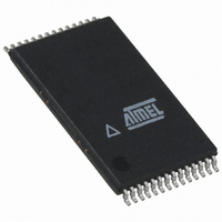
IC FLASH 32MBIT 40MHZ 28TSOP
Manufacturer
Atmel
Datasheet
1.AT45DB321C-RU.pdf
(40 pages)
Specifications of AT45DB321C-TC
Format - Memory
FLASH
Memory Type
DataFLASH
Memory Size
32M (8192 pages x 528 bytes)
Speed
40MHz
Interface
SPI, 3-Wire Serial
Voltage - Supply
2.7 V ~ 3.6 V
Operating Temperature
0°C ~ 70°C
Package / Case
28-TSOP
Lead Free Status / RoHS Status
Contains lead / RoHS non-compliant


10. Electrical Specifications
Table 10-1.
Table 10-2.
Note:
Table 10-3.
Notes:
3387M–DFLASH–2/08
Temperature under Bias ............................... -55° C to +125° C
Storage Temperature .................................... -65° C to +150° C
All Input Voltages
(including NC Pins)
with Respect to Ground ...................................-0.6V to +6.25V
All Output Voltages
with Respect to Ground .............................-0.6V to V
Operating Temperature (Case)
V
Symbol
I
I
I
I
I
I
I
V
V
V
V
SB
CC1
CC2
CC3
CC4
LI
LO
CC
IL
IH
OL
OH
(1)
(2)(3)
Power Supply
1. After power is applied and V
1. I
2. I
3. I
4. All inputs are 5 volts tolerant.
tional mode is started.
SB
CC1
CC1
Parameter
Standby Current
Active Current, Read
Operation, Serial Interface
Active Current, Program
Operation, Page Program
Active Current, Page Erase
Operation
Active Current, Block Erase
Operation
Input Load Current
Output Leakage Current
Input Low Voltage
Input High Voltage
Output Low Voltage
Output High Voltage
maximum specification limit is tested at 3.3V and 70° C.
Absolute Maximum Ratings*
DC and AC Operating Range
DC Characteristics
during a buffer read is 30 mA maximum.
changes typically by 300 µA per 1 MHz change in clock frequency.
(1)
CC
is at the minimum specified datasheet value, the system should wait 20 ms before an opera-
Com.
Ind.
Condition
CS, RESET, WP = V
inputs at CMOS levels
f = 20 MHz; I
V
V
V
V
V
V
I
I
OL
OH
CC
CC
CC
CC
IN
I/O
= 1.6 mA; V
= -100 µA
= CMOS levels
= CMOS levels
= 3.6V
= 3.6V
= 3.6V
= 3.6V
CC
+ 0.6V
OUT
CC
= 0 mA;
= 2.7V
IH
, all
*NOTICE:
V
V
CC
CC
Stresses beyond those listed under “Absolute
Maximum Ratings” may cause permanent dam-
age to the device. This is a stress rating only and
functional operation of the device at these or any
other conditions beyond those indicated in the
operational sections of this specification is not
implied. Exposure to absolute maximum rating
conditions for extended periods may affect device
reliability.
Min
- 0.2V
x 0.7
-40° C to 85° C
AT45DB321C
0° C to 70° C
2.7V to 3.6V
Typ
10
35
30
30
6
AT45DB321C
V
CC
Max
0.4
15
15
50
40
40
1
1
x 0.3
Units
mA
mA
mA
mA
µA
µA
µA
V
V
V
V
21
Related parts for AT45DB321C-TC
Image
Part Number
Description
Manufacturer
Datasheet
Request
R

Part Number:
Description:
DEV KIT FOR AVR/AVR32
Manufacturer:
Atmel
Datasheet:

Part Number:
Description:
INTERVAL AND WIPE/WASH WIPER CONTROL IC WITH DELAY
Manufacturer:
ATMEL Corporation
Datasheet:
Part Number:
Description:
Low-Voltage Voice-Switched IC for Hands-Free Operation
Manufacturer:
ATMEL Corporation
Datasheet:
Part Number:
Description:
MONOLITHIC INTEGRATED FEATUREPHONE CIRCUIT
Manufacturer:
ATMEL Corporation
Datasheet:
Part Number:
Description:
AM-FM Receiver IC U4255BM-M
Manufacturer:
ATMEL Corporation
Datasheet:
Part Number:
Description:
Monolithic Integrated Feature Phone Circuit
Manufacturer:
ATMEL Corporation
Datasheet:
Part Number:
Description:
Multistandard Video-IF and Quasi Parallel Sound Processing
Manufacturer:
ATMEL Corporation
Datasheet:
Part Number:
Description:
High-performance EE PLD
Manufacturer:
ATMEL Corporation
Datasheet:
Part Number:
Description:
8-bit Flash Microcontroller
Manufacturer:
ATMEL Corporation
Datasheet:
Part Number:
Description:
2-Wire Serial EEPROM
Manufacturer:
ATMEL Corporation
Datasheet: