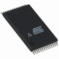
AT45DB321C-TC Atmel, AT45DB321C-TC Datasheet - Page 14

AT45DB321C-TC
Manufacturer Part Number
AT45DB321C-TC
Description
IC FLASH 32MBIT 40MHZ 28TSOP
Manufacturer
Atmel
Datasheet
1.AT45DB321C-RU.pdf
(40 pages)
Specifications of AT45DB321C-TC
Format - Memory
FLASH
Memory Type
DataFLASH
Memory Size
32M (8192 pages x 528 bytes)
Speed
40MHz
Interface
SPI, 3-Wire Serial
Voltage - Supply
2.7 V ~ 3.6 V
Operating Temperature
0°C ~ 70°C
Package / Case
28-TSOP
Lead Free Status / RoHS Status
Contains lead / RoHS non-compliant
7.2
7.3
14
Security Register
Operation Mode Summary
AT45DB321C
The AT45DB321C contains a specialized register that can be used for security purposes in sys-
tem design. The Security Register is a unique 128-byte register that is divided into two portions.
The first 64 bytes (byte 0 to byte 63) of this page are allocated as a one-time user programmable
space. Once these 64 bytes have been programmed, they should not be reprogrammed. The
remaining 64 bytes of this page (byte 64 to byte 127) are factory programmed by Atmel and will
contain a unique number for each device. The factory programmed data is fixed and cannot be
changed.
The Security Register can be read by clocking in a 4-byte sequence 77H, 00H, 00H, 00H to the
device followed by 32 don’t care clock cycles. See the opcode
Note:
To program the first 64 bytes of the Security Register, a two step sequence must be used. The
first step requires that the user loads the desired data into Buffer 1 by using the Buffer 1 Write
operation (opcode 84H –
address as location zero and should write a full 64 bytes of information into the buffer. Other-
wise, the first 64 bytes of the buffer may contain data that was previously stored in the buffer. It
is not necessary to fill the remaining 464 bytes (byte locations 64 through 527) of the buffer with
data. After the Buffer 1 Write operation has been completed, the Security Register can be sub-
sequently programmed by reselecting the device and clocking in opcode 9AH into the device
followed by three don’t care bytes (24 clock cycles). After the final don’t care clock cycle has
been completed, a low-to-high transition on the CS pin will cause the device to initiate an inter-
nally self-timed program operation in which the contents of Buffer 1 will be programmed into the
Security Register. Only the first 64 bytes of data in Buffer 1 will be programmed into the Security
Register; the remaining 464 bytes of the buffer will be ignored. The Security Register program
operation should take place in a maximum time of t
The modes described can be separated into two groups – modes that make use of the Flash
memory array (Group A) and modes that do not make use of the Flash memory array (Group B).
Group A modes consist of:
Group B modes consist of:
1. Main Memory Page Read
2. Continuous Array Read
3. Main Memory Page to Buffer 1 (or 2) Transfer
4. Main Memory Page to Buffer 1 (or 2) Compare
5. Buffer 1 (or 2) to Main Memory Page Program with Built-in Erase
6. Buffer 1 (or 2) to Main Memory Page Program without Built-in Erase
7. Main Memory Page Program through Buffer 1 (or 2)
8. Page Erase
9. Block Erase
10. Auto Page Rewrite
1. Buffer 1 (or 2) Read
2. Buffer 1 (or 2) Write
3. Status Register Read
4. Manufacturer and Device ID Read
Next generation devices of the “D” family will not require the 32 don’t care clock cycles.
“Buffer Write” on page
5). The user should specify the starting buffer
P
.
Table 9-4 on page
3387M–DFLASH–2/08
20.


