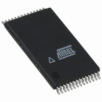
AT45DB321C-TC Atmel, AT45DB321C-TC Datasheet - Page 17

AT45DB321C-TC
Manufacturer Part Number
AT45DB321C-TC
Description
IC FLASH 32MBIT 40MHZ 28TSOP
Manufacturer
Atmel
Datasheet
1.AT45DB321C-RU.pdf
(40 pages)
Specifications of AT45DB321C-TC
Format - Memory
FLASH
Memory Type
DataFLASH
Memory Size
32M (8192 pages x 528 bytes)
Speed
40MHz
Interface
SPI, 3-Wire Serial
Voltage - Supply
2.7 V ~ 3.6 V
Operating Temperature
0°C ~ 70°C
Package / Case
28-TSOP
Lead Free Status / RoHS Status
Contains lead / RoHS non-compliant
8. Power-on/Reset State
9. System Considerations
3387M–DFLASH–2/08
When power is first applied to the device, or when recovering from a reset condition, the device
will default to Mode 3. In addition, the output pin (SO) will be in a high impedance state, and a
high-to-low transition on the CS pin will be required to start a valid instruction. The mode (Mode
3 or Mode 0) will be automatically selected on every falling edge of CS by sampling the inactive
clock state. After power is applied and V
should wait 20 ms before an operational mode (DataFlash) is started.
The RapidS serial interface is controlled by the serial clock SCK, serial input SI and chip select
CS pins. These signals must rise and fall monotonically and be free from noise. Excessive noise
or ringing on these pins can be misinterpreted as multiple edges and cause improper operation
of the device. The PC board traces must be kept to a minimum distance or appropriately termi-
nated to ensure proper operation. If necessary, decoupling capacitors can be added on these
pins to provide filtering against noise glitches.
As system complexity continues to increase, voltage regulation is becoming more important.
A key element of any voltage regulation scheme is its current sourcing capability. Like all Flash
memories, the peak current for DataFlash occur during the programming and erase operation.
The regulator needs to supply this peak current requirement. An under specified regulator can
cause current starvation. Besides increasing system noise, current starvation during program-
ming or erase can lead to improper operation and possible data corruption.
For applications that require random modifications of data within a sector, please refer to
Page Rewrite” on page
Atmel C generation DataFlash utilizes a sophisticated adaptive algorithm during erase and pro-
gramming to maximize the endurance over the life of the device. The algorithm uses a
verification mechanism to check if the memory cells have been erased or programmed success-
fully. If the memory cells were not erased or programmed completely, the algorithm erases or
programs the memory cells again. The process will continue until the device is erased or pro-
grammed successfully.
In order to optimize the erase and programming time, fixed timing should not be used.
Instead, the RDY/BUSY bit of the status register or the RDY/BUSY pin should be
monitored.
8.
CC
is at the minimum datasheet value, the system
AT45DB321C
“Auto
17


