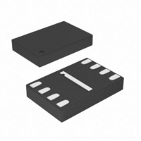
M95640-RMB6TG STMicroelectronics, M95640-RMB6TG Datasheet - Page 26

M95640-RMB6TG
Manufacturer Part Number
M95640-RMB6TG
Description
IC EEPROM 64KBIT 2MHZ 8MLP
Manufacturer
STMicroelectronics
Specifications of M95640-RMB6TG
Format - Memory
EEPROMs - Serial
Memory Type
EEPROM
Memory Size
64K (8K x 8)
Speed
2MHz
Interface
SPI, 3-Wire Serial
Voltage - Supply
1.8 V ~ 5.5 V
Operating Temperature
-40°C ~ 85°C
Package / Case
8-MLP
Memory Configuration
8192 X 8
Interface Type
Serial, SPI
Clock Frequency
2MHz
Supply Voltage Range
1.8V To 5.5V
Memory Case Style
DFN
No. Of Pins
8
Rohs Compliant
Yes
Lead Free Status / RoHS Status
Lead free / RoHS Compliant
Other names
M95640-RMB6TGCT
Available stocks
Company
Part Number
Manufacturer
Quantity
Price
Part Number:
M95640-RMB6TG
Manufacturer:
ST
Quantity:
20 000
Instructions
6.8
6.9
26/48
Write Identification Page
The Identification Page (32 bytes) is an additional page which can be written and (later)
permanently locked in Read-only mode. Writing this page is achieved with the Write
Identification Page instruction (see
bits of the instruction byte, address byte, and at least one data byte are then shifted in on
Serial Data input (D). Address bit A10 must be 0, address bits [A15:A11] and [A9:A5] are
Don't Care, the [A4:A0] address bits define the byte address inside the identification page.
Figure 15. Write Identification Page sequence
Read Lock Status
The Read Lock Status instruction is used to read the lock status. To send this instruction to
the device, Chip Select (S) first has to be driven low. The bits of the instruction byte and
address bytes are then shifted in on Serial Data input (D). Address bit A10 must be 1, all
other address bits are Don't Care. The Lock bit is the LSB (least significant bit) of the byte
read on Serial Data output (Q). It is at ‘1’ when the lock is active and at ‘0’ when the lock is
not active. If Chip Select (S) continues to be driven low, the same data byte is shifted out.
The read cycle is terminated by driving Chip Select (S) high. The instruction sequence is
shown in
Figure
16.
Doc ID 16877 Rev 15
Table
4), the Chip Select signal (S) is first driven low. The
M95640, M95640-W, M95640-R, M95640-DR


