CY7C1049DV33-10VXIT Cypress Semiconductor Corp, CY7C1049DV33-10VXIT Datasheet
CY7C1049DV33-10VXIT
Specifications of CY7C1049DV33-10VXIT
Available stocks


Related parts for CY7C1049DV33-10VXIT


CY7C1049DV33-10VXIT Summary of contents
Page 1
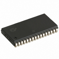
... HIGH), the outputs are disabled (OE HIGH), or during a write operation (CE LOW, and WE LOW). The CY7C1049DV33 is available in standard 400 Mil wide 36 -pin SOJ package and 44-pin TSOP II package with center power and ground (revolutionary) pinout. INPUT BUFFER ...
Page 2
... Capacitance ...................................................................... 4 Thermal Resistance .......................................................... 5 AC Test Loads and Waveforms ....................................... 5 Data Retention Characteristics ....................................... 5 AC Switching Characteristics ......................................... 6 Switching Waveforms ...................................................... 7 Truth Table ........................................................................ 9 Document Number: 38-05475 Rev. *G CY7C1049DV33 Ordering Information ........................................................ 9 Ordering Code Definitions ........................................... 9 Package Diagrams .......................................................... 10 Acronyms ........................................................................ 12 Document Conventions ................................................. 12 Units of Measure ....................................................... 12 Document History Page ................................................. 13 Sales, Solutions, and Legal Information ...................... 14 Worldwide Sales and Design Support ...
Page 3
... Pin Configuration 36-pin SOJ Top View GND Selection Guide Maximum Access Time Maximum Operating Current Maximum CMOS Standby Current Note 1. Automotive product information is preliminary. Document Number: 38-05475 Rev. *G 44-pin TSOP II Top View GND -10 (Industrial) -12 (Automotive CY7C1049DV33 [1] Unit Page [+] Feedback ...
Page 4
... IH < MAX , CE > V – 0.3 V, – > V – 0 < 0 Test Conditions = 25 MHz 3 CY7C1049DV33 Ambient Temperature V Speed CC –40 C to +85 C 3.3 V 0 –40 C to +125 C 3.3 V 0 -12 (Automotive) Max Min Max – 2.4 – 0.4 – 0 0.3 2 ...
Page 5
... V > CDR Figure 1 (a). High Z characteristics are tested for all speeds using the test load shown > 50 s or stable at V > 50 CC(min.) CC(min.) CY7C1049DV33 36-pin SOJ 44-pin TSOP II Package Package 57.91 50.66 36.73 17.17 [4] ALL INPUT PULSES 90% 90% 10% ...
Page 6
... CC is less than less than t , and t is less than t LZCE HZOE LZOE HZWE Figure 1 on page 5. Transition is measured when the outputs enter a high impedance state. and t HZWE CY7C1049DV33 -12 (Automotive) Max Min Max – 100 – – 12 – 10 – 12 – ...
Page 7
... If CE goes HIGH simultaneously with WE going HIGH, the output remains in a high impedance state. Document Number: 38-05475 Rev. *G [13, 14] Figure 3. Read Cycle No OHA DOE DATA VALID 50 SCE PWE t SD DATA VALID IN CY7C1049DV33 DATA VALID [14, 15] t HZOE t HZCE HIGH IMPEDANCE 50 [16, 17 Page [+] Feedback ...
Page 8
... If CE goes HIGH simultaneously with WE going HIGH, the output remains in a high impedance state. 19. During this period the IOs are in the output state and input signals must not be applied. 20. Data IO is high impedance Document Number: 38-05475 Rev SCE PWE t SD DATA VALID SCE SCE PWE t SD DATA VALID CY7C1049DV33 [18 LZWE [18, 20 Page [+] Feedback ...
Page 9
... Temperature Range Industrial E = Automotive-E Pb-free Package Type 36-pin (400-Mil) Molded SOJ ZS = 44-pin TSOP II Speed V33 = Voltage range ( 3 C9 Technology 9 = Data width × 8-bits 04 = 4-Mbit density 1 = Fast Asynchronous SRAM family Technology Code CMOS 7 = SRAM CY = Cypress CY7C1049DV33 Mode Power Standby ( Active ( Active ( Active ( Operating ...
Page 10
... Package Diagrams Figure 8. 36-pin (400-Mil) Molded SOJ V36.4, (51-85090) Document Number: 38-05475 Rev. *G CY7C1049DV33 51-85090 *E Page [+] Feedback ...
Page 11
... Package Diagrams (continued) Document Number: 38-05475 Rev. *G Figure 9. 44-pin TSOP Z44-II, (51-85087) CY7C1049DV33 51-85087 *C Page [+] Feedback ...
Page 12
... SOJ small outline J-lead SRAM static random access memory TSOP thin small outline package TTL transistor-transistor logic WE write enable Document Number: 38-05475 Rev. *G CY7C1049DV33 Document Conventions Units of Measure Symbol Unit of Measure °C degree Celcius MHz Mega Hertz µA micro Amperes µs ...
Page 13
... Document History Page Document Title: CY7C1049DV33, 4-Mbit (512 K × 8) Static RAM Document Number: 38-05475 Orig. of REV. ECN NO. Issue Date Change ** 201560 See ECN *A 233729 See ECN *B 351096 See ECN *C 446328 See ECN NXR *D 1274726 See ECN VKN/AESA Corrected typo in the 44-Pin TSOP II pinout ...
Page 14
... Cypress against all charges. Use may be limited by and subject to the applicable Cypress software license agreement. Document Number: 38-05475 Rev. *G All products and company names mentioned in this document may be the trademarks of their respective holders. cypress.com/go/plc Revised June 1, 2011 CY7C1049DV33 PSoC Solutions psoc.cypress.com/solutions PSoC 1 | PSoC 3 ...