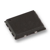
M45PE80-VMP6G NUMONYX, M45PE80-VMP6G Datasheet - Page 46

M45PE80-VMP6G
Manufacturer Part Number
M45PE80-VMP6G
Description
IC FLASH 8MBIT 50MHZ 8VFQFPN
Manufacturer
NUMONYX
Series
Forté™r
Datasheet
1.M45PE80-VMP6G.pdf
(48 pages)
Specifications of M45PE80-VMP6G
Format - Memory
FLASH
Memory Type
FLASH
Memory Size
8M (1M x 8)
Speed
50MHz
Interface
SPI, 3-Wire Serial
Voltage - Supply
2.7 V ~ 3.6 V
Operating Temperature
-40°C ~ 85°C
Package / Case
8-VFQFN, 8-VFQFPN
Ic Interface Type
Serial, SPI
Clock Frequency
75MHz
Supply Voltage Range
2.7V To 3.6V
No. Of Pins
8
Operating Temperature Range
-40°C To +85°C
Voltage, Vcc
3V
Rohs Compliant
Yes
Lead Free Status / RoHS Status
Lead free / RoHS Compliant
Available stocks
Company
Part Number
Manufacturer
Quantity
Price
Company:
Part Number:
M45PE80-VMP6G
Manufacturer:
MICROCHIP
Quantity:
3 000
Company:
Part Number:
M45PE80-VMP6G
Manufacturer:
Micron Technology Inc
Quantity:
10 000
Part Number:
M45PE80-VMP6G
Manufacturer:
MICRON/美光
Quantity:
20 000
Company:
Part Number:
M45PE80-VMP6G-N
Manufacturer:
STMicroelectronics
Quantity:
500
13
14
46/48
Reference
Revision history
Table 22.
05-May-2003
28-May-2004
10-May-2005
10-Feb-2003
26-Nov-2003
14-Feb-2006
02-Apr-2003
08-Apr-2003
04-Jun-2003
23-Jan-2004
4-Oct-2005
AN1995: Serial Flash Memory Device Marking.
Date
Document revision history
Version
1.0
1.1
1.2
1.3
1.4
2.0
3.0
4.0
5.0
6.0
7
Document written
VFQFPN8 (MLP) package added
Document promoted to Product Preview
Document promoted to Preliminary Data
Description corrected of entering Hardware Protected mode (W must be
driven, and cannot be left unconnected). Document Revision History for
05-May-2003 corrected.
V
contents, SO16 package, warning about exposed paddle on MLP8, and
Pb-free options added. Change of naming for VDFPN8 package.
Document promoted to full datasheet
SO16 pin-out corrected
Soldering temperature information clarified for RoHS compliant devices.
Device Grade clarified
SO16 wide package replaced by SO8 wide package.
Active Power, Stand-by Power and Deep Power-Down
Identification
Power-down (RDP)
Table 21: Ordering information scheme
Figure 22: Output timing
Added
modify
Program (PP)
Page Program instructions. Updated I
characteristics. Updated
information added.
X process technology added (see
Reset timings for U process technology devices
timings for X process technology
VFQFPN8, MLP silhouette modified
Table 7: Absolute maximum
Table 5: Status Register Format
to
under
IO
Section 6.4: Read Status Register
(min) extended to –0.6V, and t
Plating Technology
Table 12: AC characteristics (33 MHz
data,
A fast way to modify
(RDID),
sections updated to explain optimal use of Page Write and
descriptions updated.
Deep Power-down
updated.
Table 21: Ordering information scheme
in
ratings.
Table 21: Ordering information
Changes
moved from
devices). MLP package renamed as
PP
data,
Section 2.5: Reset
(typ) improved to 1.2ms. Table of
on page
(RDSR). Blank option removed
CC3
Page Write (PW)
updated.
(DP), and
values in
Section 4.7: Status Register
operation).
1. T
and
LEAD
Release from Deep
Table 11: DC
Table 15: Reset
(Reset),
removed from
modes,
An easy way to
and
scheme.
Page
Table 14:
Read
RoHS


