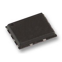
M45PE80-VMP6G NUMONYX, M45PE80-VMP6G Datasheet - Page 21

M45PE80-VMP6G
Manufacturer Part Number
M45PE80-VMP6G
Description
IC FLASH 8MBIT 50MHZ 8VFQFPN
Manufacturer
NUMONYX
Series
Forté™r
Datasheet
1.M45PE80-VMP6G.pdf
(48 pages)
Specifications of M45PE80-VMP6G
Format - Memory
FLASH
Memory Type
FLASH
Memory Size
8M (1M x 8)
Speed
50MHz
Interface
SPI, 3-Wire Serial
Voltage - Supply
2.7 V ~ 3.6 V
Operating Temperature
-40°C ~ 85°C
Package / Case
8-VFQFN, 8-VFQFPN
Ic Interface Type
Serial, SPI
Clock Frequency
75MHz
Supply Voltage Range
2.7V To 3.6V
No. Of Pins
8
Operating Temperature Range
-40°C To +85°C
Voltage, Vcc
3V
Rohs Compliant
Yes
Lead Free Status / RoHS Status
Lead free / RoHS Compliant
Available stocks
Company
Part Number
Manufacturer
Quantity
Price
Company:
Part Number:
M45PE80-VMP6G
Manufacturer:
MICROCHIP
Quantity:
3 000
Company:
Part Number:
M45PE80-VMP6G
Manufacturer:
Micron Technology Inc
Quantity:
10 000
Part Number:
M45PE80-VMP6G
Manufacturer:
MICRON/美光
Quantity:
20 000
Company:
Part Number:
M45PE80-VMP6G-N
Manufacturer:
STMicroelectronics
Quantity:
500
6.5
Figure 9.
Read Data Bytes (READ)
The device is first selected by driving Chip Select (S) Low. The instruction code for the Read
Data Bytes (READ) instruction is followed by a 3-byte address (A23-A0), each bit being
latched-in during the rising edge of Serial Clock (C). Then the memory contents at that
address is shifted out on Serial Data Output (Q), each bit being shifted out at a maximum
frequency f
in
The first byte addressed can be at any location. The address is automatically incremented
to the next higher address after each byte of data is shifted out. The whole memory can,
therefore, be read with a single Read Data Bytes (READ) instruction. When the highest
address is reached, the address counter rolls over to 000000h, allowing the read sequence
to be continued indefinitely.
The Read Data Bytes (READ) instruction is terminated by driving Chip Select (S) High. Chip
Select (S) can be driven High at any time during data output. Any Read Data Bytes (READ)
instruction, while an Erase, Program or Write cycle is in progress, is rejected without having
any effects on the cycle that is in progress.
Figure
S
C
D
Q
10.
R
, during the falling edge of Serial Clock (C). The instruction sequence is shown
Read Status Register (RDSR) instruction sequence and data-out
sequence
0
High Impedance
1
2
Instruction
3
4
5
6
7
MSB
7
8
6
Status Register Out
9 10 11 12 13 14 15
5
4
3
2
1
0
MSB
7
6
Status Register Out
5
4
3
2
1
0
7
AI02031E
21/48


