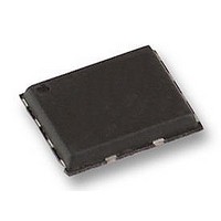
M45PE80-VMP6G NUMONYX, M45PE80-VMP6G Datasheet - Page 23

M45PE80-VMP6G
Manufacturer Part Number
M45PE80-VMP6G
Description
IC FLASH 8MBIT 50MHZ 8VFQFPN
Manufacturer
NUMONYX
Series
Forté™r
Datasheet
1.M45PE80-VMP6G.pdf
(48 pages)
Specifications of M45PE80-VMP6G
Format - Memory
FLASH
Memory Type
FLASH
Memory Size
8M (1M x 8)
Speed
50MHz
Interface
SPI, 3-Wire Serial
Voltage - Supply
2.7 V ~ 3.6 V
Operating Temperature
-40°C ~ 85°C
Package / Case
8-VFQFN, 8-VFQFPN
Ic Interface Type
Serial, SPI
Clock Frequency
75MHz
Supply Voltage Range
2.7V To 3.6V
No. Of Pins
8
Operating Temperature Range
-40°C To +85°C
Voltage, Vcc
3V
Rohs Compliant
Yes
Lead Free Status / RoHS Status
Lead free / RoHS Compliant
Available stocks
Company
Part Number
Manufacturer
Quantity
Price
Company:
Part Number:
M45PE80-VMP6G
Manufacturer:
MICROCHIP
Quantity:
3 000
Company:
Part Number:
M45PE80-VMP6G
Manufacturer:
Micron Technology Inc
Quantity:
10 000
Part Number:
M45PE80-VMP6G
Manufacturer:
MICRON/美光
Quantity:
20 000
Company:
Part Number:
M45PE80-VMP6G-N
Manufacturer:
STMicroelectronics
Quantity:
500
6.7
Figure 11. Read Data Bytes at Higher Speed (FAST_READ) instruction sequence
1. Address bits A23 to A20 are Don’t Care.
Page Write (PW)
The Page Write (PW) instruction allows bytes to be written in the memory. Before it can be
accepted, a Write Enable (WREN) instruction must previously have been executed. After
the Write Enable (WREN) instruction has been decoded, the device sets the Write Enable
Latch (WEL).
The Page Write (PW) instruction is entered by driving Chip Select (S) Low, followed by the
instruction code, three address bytes and at least one data byte on Serial Data Input (D).
The rest of the page remains unchanged if no power failure occurs and the device is not
reset during the write cycle.
The Page Write (PW) instruction performs a page erase cycle even if only one byte is
updated.
If the 8 least significant address bits (A7-A0) are not all zero, all transmitted data exceeding
the addressed page boundary roll over, and are written from the start address of the same
page (the one whose 8 least significant address bits (A7-A0) are all zero). Chip Select (S)
must be driven Low for the entire duration of the sequence.
The instruction sequence is shown in
S
C
D
Q
S
C
D
Q
0
and data-out sequence
7
1
32 33 34
High Impedance
6
2
Instruction
Dummy Byte
5
3
4
35
4
3
36 37 38 39 40 41 42 43 44 45 46
5
2
6
1
7
23
0
8
MSB
22 21
7
9 10
24 BIT ADDRESS
Figure
6
DATA OUT 1
5
12.
3
28 29 30 31
4
2
3
1
2
0
1
0
47
MSB
7
6
DATA OUT 2
5
4
3
2
1
0
MSB
7
AI04006
23/48


