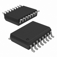
AT25DF641-S3H-T Atmel, AT25DF641-S3H-T Datasheet - Page 39

AT25DF641-S3H-T
Manufacturer Part Number
AT25DF641-S3H-T
Description
IC FLASH 64MBIT 100MHZ 16SOIC
Manufacturer
Atmel
Datasheet
1.AT25DF641-MWH-T.pdf
(56 pages)
Specifications of AT25DF641-S3H-T
Format - Memory
FLASH
Memory Type
DataFLASH
Memory Size
64M (32K pages x 256 bytes)
Speed
100MHz
Interface
SPI, 3-Wire Serial
Voltage - Supply
2.7 V ~ 3.6 V
Operating Temperature
-40°C ~ 85°C
Package / Case
16-SOIC (0.300", 7.5mm Width)
Lead Free Status / RoHS Status
Lead free / RoHS Compliant
Available stocks
Company
Part Number
Manufacturer
Quantity
Price
Part Number:
AT25DF641-S3H-T
Manufacturer:
ATMEL/爱特梅尔
Quantity:
20 000
10.3.
3680F–DFLASH–4/10
Write Status Register Byte 2
The Write Status Register Byte 2 command is used to modify the RSTE and SLE bits of the Status Register.
Using the Write Status Register Byte 2 command is the only way to modify the RSTE and SLE bits in the Status
Register during normal device operation, and the SLE bit can only be modified if the sector lockdown state has
not been frozen. Before the Write Status Register Byte 2 command can be issued, the Write Enable command
must have been previously issued to set the WEL bit in the Status Register to a logical “1”.
To issue the Write Status Register Byte 2 command, the
must be clocked into the device followed by one byte of data. The one byte of data consists of three don’t care
bits, the RSTE bit value, the SLE bit value, and three additional don’t care bits (see Table 10-1). Any additional
data bytes that are sent to the device will be ignored. When the
the Status Register will be modified, and the WEL bit in the Status Register will be reset back to a logical “0”. The
SLE bit will only be modified if the Freeze Sector Lockdown State command has not been previously issued.
The complete one byte of data must be clocked into the device before the
must be deasserted on even byte boundaries (multiples of eight bits); otherwise, the device will abort the
operation, the state of the RSTE and SLE bits will not change, and the WEL bit in the Status Register will be reset
back to the logical “0” state.
Table 10-4.
Figure 10-3. Write Status Register Byte 2
SCK
SO
CS
Bit 7
SI
X
Write Status Register Byte 2 Format
Bit 6
X
MS B
HIG H-IMP E DANC E
0
0
0
1
1
2
OPCODE
Bit 5
1
X
3
0
4
0
5
0
6
RSTE
1
Bit 4
7
MS B
X
8
S TATUS R E GIS TE R IN
X
9
X
10 11
BYTE 2
D
Bit 3
SLE
D
12
X
13
X
14 15
X
CS
Bit 2
pin must first be asserted and the opcode of 31h
X
CS
pin is deasserted, the RSTE and SLE bits in
Bit 1
X
CS
Atmel AT25DF641
pin is deasserted, and the
Bit 0
X
CS
pin
39


