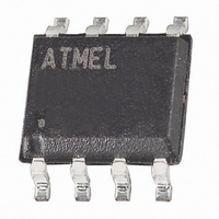
AT25DF321A-SH-T Atmel, AT25DF321A-SH-T Datasheet - Page 6

AT25DF321A-SH-T
Manufacturer Part Number
AT25DF321A-SH-T
Description
IC FLASH 32MBIT 100MHZ 8SOIC
Manufacturer
Atmel
Datasheet
1.AT25DF321A-SH-T.pdf
(51 pages)
Specifications of AT25DF321A-SH-T
Format - Memory
FLASH
Memory Type
DataFLASH
Memory Size
32M (16384 pages x 256 Bytes)
Speed
100MHz
Interface
SPI, RapidS
Voltage - Supply
2.7 V ~ 3.6 V
Operating Temperature
-40°C ~ 85°C
Package / Case
8-SOIC (5.3mm Width), 8-SOP, 8-SOEIAJ
Density
32Mb
Access Time (max)
5ns
Interface Type
Serial (SPI)
Address Bus
1b
Operating Supply Voltage (typ)
3.3V
Operating Temp Range
-40C to 85C
Package Type
SOIC
Program/erase Volt (typ)
2.7 to 3.6V
Sync/async
Synchronous
Operating Temperature Classification
Industrial
Operating Supply Voltage (min)
2.7V
Operating Supply Voltage (max)
3.6V
Word Size
8b
Number Of Words
4M
Supply Current
19mA
Mounting
Surface Mount
Pin Count
8
Lead Free Status / RoHS Status
Lead free / RoHS Compliant
Available stocks
Company
Part Number
Manufacturer
Quantity
Price
Company:
Part Number:
AT25DF321A-SH-T
Manufacturer:
CYPRESS
Quantity:
1 872
Part Number:
AT25DF321A-SH-T
Manufacturer:
ATMEL/爱特梅尔
Quantity:
20 000
5.
6.
6
Device Operation
The Atmel
the SPI Master. The SPI Master communicates with the AT25DF321A via the SPI bus which is comprised of four signal
lines: Chip Select (CS), Serial Clock (SCK), Serial Input (SI), and Serial Output (SO).
The AT25DF321A features a dual-input program mode in which the SO pin becomes an input. Similarly, the device also
features a dual-output read mode in which the SI pin becomes an output. In the Dual-Input Byte/Page Program command
description, the SO pin will be referred to as the SOI (Serial Output/Input) pin, and in the Dual-Output Read Array
command, the SI pin will be referenced as the SIO (Serial Input/Output) pin.
The SPI protocol defines a total of four modes of operation (mode 0, 1, 2, or 3) with each mode differing in respect to the
SCK polarity and phase and how the polarity and phase control the flow of data on the SPI bus. The AT25DF321A supports
the two most common modes, SPI Modes 0 and 3. The only difference between SPI Modes 0 and 3 is the polarity of the
SCK signal when in the inactive state (when the SPI Master is in standby mode and not transferring any data). With SPI
Modes 0 and 3, data is always latched in on the rising edge of SCK and always output on the falling edge of SCK.
Figure 5-1.
Commands and Addressing
A valid instruction or operation must always be started by first asserting the CS pin. After the CS pin has been asserted, the
host controller must then clock out a valid 8-bit opcode on the SPI bus. Following the opcode, instruction dependent
information such as address and data bytes would then be clocked out by the host controller. All opcode, address, and data
bytes are transferred with the most-significant bit (MSB) first. An operation is ended by deasserting the CS pin.
Opcodes not supported by the AT25DF321A will be ignored by the device and no operation will be started. The device will
continue to ignore any data presented on the SI pin until the start of the next operation (CS pin being deasserted and then
reasserted). In addition, if the CS pin is deasserted before complete opcode and address information is sent to the device,
then no operation will be performed and the device will simply return to the idle state and wait for the next operation.
Addressing of the device requires a total of three bytes of information to be sent, representing address bits A23-A0. Since
the upper address limit of the AT25DF321A memory array is 3FFFFFh, address bits A23-A22 are always ignored by the
device.
SCK
Atmel AT25DF321A
SO
CS
SI
®
AT25DF321A is controlled by a set of instructions that are sent from a host controller, commonly referred to as
SPI Mode 0 and 3
MSB
LSB
MSB
LSB
3686D–DFLASH–12/09


