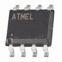
AT25DF321A-SH-T Atmel, AT25DF321A-SH-T Datasheet - Page 30

AT25DF321A-SH-T
Manufacturer Part Number
AT25DF321A-SH-T
Description
IC FLASH 32MBIT 100MHZ 8SOIC
Manufacturer
Atmel
Datasheet
1.AT25DF321A-SH-T.pdf
(51 pages)
Specifications of AT25DF321A-SH-T
Format - Memory
FLASH
Memory Type
DataFLASH
Memory Size
32M (16384 pages x 256 Bytes)
Speed
100MHz
Interface
SPI, RapidS
Voltage - Supply
2.7 V ~ 3.6 V
Operating Temperature
-40°C ~ 85°C
Package / Case
8-SOIC (5.3mm Width), 8-SOP, 8-SOEIAJ
Density
32Mb
Access Time (max)
5ns
Interface Type
Serial (SPI)
Address Bus
1b
Operating Supply Voltage (typ)
3.3V
Operating Temp Range
-40C to 85C
Package Type
SOIC
Program/erase Volt (typ)
2.7 to 3.6V
Sync/async
Synchronous
Operating Temperature Classification
Industrial
Operating Supply Voltage (min)
2.7V
Operating Supply Voltage (max)
3.6V
Word Size
8b
Number Of Words
4M
Supply Current
19mA
Mounting
Surface Mount
Pin Count
8
Lead Free Status / RoHS Status
Lead free / RoHS Compliant
Available stocks
Company
Part Number
Manufacturer
Quantity
Price
Company:
Part Number:
AT25DF321A-SH-T
Manufacturer:
CYPRESS
Quantity:
1 872
Part Number:
AT25DF321A-SH-T
Manufacturer:
ATMEL/爱特梅尔
Quantity:
20 000
11.
11.1
30
Status Register Commands
Read Status Register
The two-byte Status Register can be read to determine the device’s ready/busy status, as well as the status of many other
functions such as Hardware Locking and Software Protection. The Status Register can be read at any time, including during
an internally self-timed program or erase operation.
To read the Status Register, the CS pin must first be asserted and the opcode of 05h must be clocked into the device. After
the opcode has been clocked in, the device will begin outputting Status Register data on the SO pin during every
subsequent clock cycle. After the second byte of the Status Register has been clocked out, the sequence will repeat itself
starting again with the first byte of the Status Register as long as the CS pin remains asserted and the clock pin is being
pulsed. The data in the Status Register is constantly being updated, so each repeating sequence will output new data. The
RDY/BSY status is available for both bytes of the Status Register and is updated for each byte.
At clock frequencies above f
operating at clock frequencies above f
the correct values of both bytes of the Status Register.
Deasserting the CS pin will terminate the Read Status Register operation and put the SO pin into a high-impedance state.
The CS pin can be deasserted at any time and does not require that a full byte of data be read.
Table 11-1.
Notes:
Bit
Atmel AT25DF321A
3:2
7
6
5
4
1
0
(1)
1. Only bit 7 of Status Register Byte 1 will be modified when using the Write Status Register Byte 1 command
2. R/W = Readable and writeable
RDY/BSY
SPRL
WPP
SWP
WEL
R = Readable only
RES
EPE
Status Register Format – Byte 1
Sector Protection Registers Locked
Reserved for future use
Erase/Program Error
Write Protect (WP) Pin Status
Software Protection Status
Write Enable Latch Status
Ready/Busy Status
CLK
Name
, the first two bytes of data output from the Status Register will not be valid. Therefore, if
CLK
, at least four bytes of data must be clocked out from the device in order to read
Type
R/W
R
R
R
R
R
R
(2)
00
01
10
11
0
1
0
0
1
0
1
0
1
0
1
Sector Protection Registers are unlocked (default)
Sector Protection Registers are locked
Reserved for future use
Erase or program operation was successful
Erase or program error detected
WP is asserted
WP is deasserted
All sectors are software unprotected (all Sector
Protection Registers are 0)
Some sectors are software protected. Read
individual Sector Protection Registers to determine
which sectors are protected
Reserved for future use
All sectors are software protected (all Sector
Protection Registers are 1 – default)
Device is not write enabled (default)
Device is write enabled
Device is ready
Device is busy with an internal operation
Description
3686D–DFLASH–12/09


