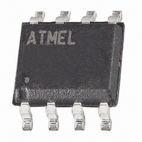
AT25DF321A-SH-T Atmel, AT25DF321A-SH-T Datasheet - Page 11

AT25DF321A-SH-T
Manufacturer Part Number
AT25DF321A-SH-T
Description
IC FLASH 32MBIT 100MHZ 8SOIC
Manufacturer
Atmel
Datasheet
1.AT25DF321A-SH-T.pdf
(51 pages)
Specifications of AT25DF321A-SH-T
Format - Memory
FLASH
Memory Type
DataFLASH
Memory Size
32M (16384 pages x 256 Bytes)
Speed
100MHz
Interface
SPI, RapidS
Voltage - Supply
2.7 V ~ 3.6 V
Operating Temperature
-40°C ~ 85°C
Package / Case
8-SOIC (5.3mm Width), 8-SOP, 8-SOEIAJ
Density
32Mb
Access Time (max)
5ns
Interface Type
Serial (SPI)
Address Bus
1b
Operating Supply Voltage (typ)
3.3V
Operating Temp Range
-40C to 85C
Package Type
SOIC
Program/erase Volt (typ)
2.7 to 3.6V
Sync/async
Synchronous
Operating Temperature Classification
Industrial
Operating Supply Voltage (min)
2.7V
Operating Supply Voltage (max)
3.6V
Word Size
8b
Number Of Words
4M
Supply Current
19mA
Mounting
Surface Mount
Pin Count
8
Lead Free Status / RoHS Status
Lead free / RoHS Compliant
Available stocks
Company
Part Number
Manufacturer
Quantity
Price
Company:
Part Number:
AT25DF321A-SH-T
Manufacturer:
CYPRESS
Quantity:
1 872
Part Number:
AT25DF321A-SH-T
Manufacturer:
ATMEL/爱特梅尔
Quantity:
20 000
3686D–DFLASH–12/09
8.2
While the device is programming, the Status Register can be read and will indicate that the device is busy. For faster
throughput, it is recommended that the Status Register be polled rather than waiting the t
data bytes have finished programming. At some point before the program cycle completes, the WEL bit in the Status
Register will be reset back to the logical “0” state.
The device also incorporates an intelligent programming algorithm that can detect when a byte location fails to program
properly. If a programming error arises, it will be indicated by the EPE bit in the Status Register.
Figure 8-1.
Figure 8-2.
Dual-Input Byte/Page Program
The Dual-Input Byte/Page Program command is similar to the standard Byte/Page Program command and can be used to
program anywhere from a single byte of data up to 256-bytes of data into previously erased memory locations. Unlike the
standard Byte/Page Program command, however, the Dual-Input Byte/Page Program command allows two bits of data to
be clocked into the device on every clock cycle rather than just one.
Before the Dual-Input Byte/Page Program command can be started, the Write Enable command must have been
previously issued to the device (see
Register to a logical “1” state. To perform a Dual-Input Byte/Page Program command, an opcode of A2h must be clocked
into the device followed by the three address bytes denoting the first byte location of the memory array to begin
programming at. After the address bytes have been clocked in, data can then be clocked into the device two bits at a time
on both the SOI and SI pins.
The data is always input with the MSB of a byte first, and the MSB is always input on the SOI pin. During the first clock
cycle, bit 7 of the first data byte would be input on the SOI pin while bit 6 of the same data byte would be input on the SI
pin. During the next clock cycle, bits 5 and 4 of the first data byte would be input on the SOI and SI pins, respectively. The
sequence would continue with each byte of data being input after every four clock cycles. Like the standard Byte/Page
Program command, all data clocked into the device is stored in an internal buffer.
SCK
SCK
SO
SO
CS
CS
SI
SI
Byte Program
Page Program
HIGH-IMPEDANCE
HIGH-IMPEDANCE
MSB
MSB
0
0
0
0
0
0
1
1
0
0
2
2
OPCODE
OPCODE
0
0
3
3
0
0
4
4
0
0
5
5
1
1
6
6
“Write Enable” on page 18
0
0
7
7
MSB
MSB
A
A
ADDRESS BITS A23-A0
8
8
A
A
9
9
ADDRESS BITS A23-A0
A
A
10 11
A
A
12
A
29 30
A
A
A
31 32
MSB
A
D
29 30
) to set the Write Enable Latch (WEL) bit of the Status
A
D
33
DATA IN BYTE 1
A
D
31 32
34
MSB
D
D
35
D
D
33
36
D
D
34
37 38
DATA IN
D
D
35
D
D
36
39
D
37 38
D
MSB
D
D
39
BP
D
DATA IN BYTE n
or t
Atmel AT25DF321A
D
PP
D
time to determine if the
D
D
D
D
11


