AT25DF161-MH-T Atmel, AT25DF161-MH-T Datasheet - Page 19
AT25DF161-MH-T
Manufacturer Part Number
AT25DF161-MH-T
Description
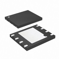
IC FLASH 16MBIT 100MHZ 8UDFN
Manufacturer
Atmel
Datasheet
1.AT25DF161-SH-B.pdf
(52 pages)
Specifications of AT25DF161-MH-T
Format - Memory
FLASH
Memory Type
DataFLASH
Memory Size
16M (2M x 8)
Speed
100MHz
Interface
SPI, RapidS
Voltage - Supply
2.7 V ~ 3.6 V
Operating Temperature
-40°C ~ 85°C
Package / Case
8-UDFN
Lead Free Status / RoHS Status
Lead free / RoHS Compliant
Available stocks
Company
Part Number
Manufacturer
Quantity
Price

Part Number:
AT25DF161-MH-T
Manufacturer:
ATMEL/爱特梅尔
Quantity:
20 000


3687E–DFLASH–11/10
9.2
9.3
Write Disable
The Write Disable command is used to reset the Write Enable Latch (WEL) bit in the Status Register to the logical "0"
state. With the WEL bit reset, all Byte/Page Program, erase, Protect Sector, Unprotect Sector, Sector Lockdown, Freeze
Sector Lockdown State, Program OTP Security Register, and Write Status Register commands will not be executed. Other
conditions can also cause the WEL bit to be reset; for more details, refer to the WEL bit section of the Status Register
description.
To issue the Write Disable command, the CS pin must first be asserted and the opcode of 04h must be clocked into the
device. No address bytes need to be clocked into the device, and any data clocked in after the opcode will be ignored.
When the CS pin is deasserted, the WEL bit in the Status Register will be reset to a logical “0”. The complete opcode must
be clocked into the device before the CS pin is deasserted, and the CS pin must be deasserted on an even byte boundary
(multiples of eight bits); otherwise, the device will abort the operation and the state of the WEL bit will not change.
Figure 9-2.
Protect Sector
Every physical 64-Kbyte sector of the device has a corresponding single-bit Sector Protection Register that is used to
control the software protection of a sector. Upon device power-up, each Sector Protection Register will default to the
logical “1” state indicating that all sectors are protected and cannot be programmed or erased.
Issuing the Protect Sector command to a particular sector address will set the corresponding Sector Protection Register to
the logical “1” state. The following table outlines the two states of the Sector Protection Registers.
Table 9-1.
Before the Protect Sector command can be issued, the Write Enable command must have been previously issued to set
the WEL bit in the Status Register to a logical “1”. To issue the Protect Sector command, the CS pin must first be asserted
and the opcode of 36h must be clocked into the device followed by three address bytes designating any address within
the sector to be protected. Any additional data clocked into the device will be ignored. When the CS pin is deasserted, the
Sector Protection Register corresponding to the physical sector addressed by A23-A0 will be set to the logical “1” state,
and the sector itself will then be protected from program and erase operations. In addition, the WEL bit in the Status
Register will be reset back to the logical “0” state.
Value
SCK
0
1
SO
CS
SI
Sector Protection Status
Sector is unprotected and can be programmed and erased.
Sector is protected and cannot be programmed or erased. This is the default state.
Write Disable
Sector Protection Register Values
Atmel AT25DF161
19
Related parts for AT25DF161-MH-T
Image
Part Number
Description
Manufacturer
Datasheet
Request
R

Part Number:
Description:
IC FLASH 16MBIT 100MHZ 8SOIC
Manufacturer:
Atmel
Datasheet:

Part Number:
Description:
8-bit Atmel Microcontrollers
Manufacturer:
ATMEL [ATMEL Corporation]
Datasheet:
Part Number:
Description:
IC FLASH 16MBIT 100MHZ 8SOIC
Manufacturer:
Atmel
Datasheet:
Part Number:
Description:
IC FLASH 16MBIT 100MHZ 8SOIC
Manufacturer:
Atmel
Datasheet:
Part Number:
Description:
IC FLASH 16MBIT 100MHZ 8SOIC
Manufacturer:
Atmel
Datasheet:

Part Number:
Description:
IC FLASH 16MBIT 100MHZ 8UDFN
Manufacturer:
Atmel
Datasheet:

Part Number:
Description:
16-megabit 2.7-volt Minimum Spi Serial Flash Memory
Manufacturer:
ATMEL Corporation
Datasheet:

Part Number:
Description:
DEV KIT FOR AVR/AVR32
Manufacturer:
Atmel
Datasheet:
Part Number:
Description:
INTERVAL AND WIPE/WASH WIPER CONTROL IC WITH DELAY
Manufacturer:
ATMEL Corporation
Datasheet:
Part Number:
Description:
Low-Voltage Voice-Switched IC for Hands-Free Operation
Manufacturer:
ATMEL Corporation
Datasheet:
Part Number:
Description:
MONOLITHIC INTEGRATED FEATUREPHONE CIRCUIT
Manufacturer:
ATMEL Corporation
Datasheet:
Part Number:
Description:
AM-FM Receiver IC U4255BM-M
Manufacturer:
ATMEL Corporation
Datasheet:
Part Number:
Description:
Monolithic Integrated Feature Phone Circuit
Manufacturer:
ATMEL Corporation
Datasheet: