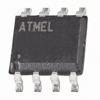
AT25DF161-SSH-T Atmel, AT25DF161-SSH-T Datasheet - Page 33

AT25DF161-SSH-T
Manufacturer Part Number
AT25DF161-SSH-T
Description
IC FLASH 16MBIT 100MHZ 8SOIC
Manufacturer
Atmel
Datasheet
1.AT25DF161-SH-B.pdf
(52 pages)
Specifications of AT25DF161-SSH-T
Format - Memory
FLASH
Memory Type
DataFLASH
Memory Size
16M (2M x 8)
Speed
100MHz
Interface
SPI, RapidS
Voltage - Supply
2.7 V ~ 3.6 V
Operating Temperature
-40°C ~ 85°C
Package / Case
8-SOIC (3.9mm Width)
Lead Free Status / RoHS Status
Lead free / RoHS Compliant
Available stocks
Company
Part Number
Manufacturer
Quantity
Price
Part Number:
AT25DF161-SSH-T
Manufacturer:
ATMEL/爱特梅尔
Quantity:
20 000
3687E–DFLASH–11/10
11.1.8 PS Bit
11.1.9 ES Bit
11.1.10 RDY/BSY Bit
11.2
execution. When the SLE bit is in the logical “1” state, the Sector Lockdown and Freeze Sector Lockdown State
commands are enabled.
Unlike the WEL bit, the SLE bit does not automatically reset after certain device operations. Therefore, once set, the SLE bit
will remain in the logical “1” state until it is modified using the Write Status Register Byte 2 command or until the device
has been power cycled. The Reset command has no effect on the SLE bit.
If the Freeze Sector Lockdown State command has been issued, then the SLE bit will be permanently reset in the logical
“0” state to indicate that the Sector Lockdown command has been disabled.
The PS bit indicates whether or not a sector is in the Program Suspend state.
The ES bit indicates whether or not a sector is in the Erase Suspend state.
The RDY/BSY bit is used to determine whether or not an internal operation, such as a program or erase, is in progress. To
poll the RDY/BSY bit to detect the completion of a program or erase cycle, new Status Register data must be continually
clocked out of the device until the state of the RDY/BSY bit changes from a logical “1” to a logical “0”.
Figure 11-1. Read Status Register
Write Status Register Byte 1
The Write Status Register Byte 1 command is used to modify the SPRL bit of the Status Register and/or to perform a
Global Protect or Global Unprotect operation. Before the Write Status Register Byte 1 command can be issued, the Write
Enable command must have been previously issued to set the WEL bit in the Status Register to a logical “1”.
To issue the Write Status Register Byte 1 command, the CS pin must first be asserted and the opcode of 01h must be
clocked into the device followed by one byte of data. The one byte of data consists of the SPRL bit value, a don’t care bit,
four data bits to denote whether a Global Protect or Unprotect should be performed, and two additional don’t care bits
(see
SPRL bit in the Status Register will be modified, and the WEL bit in the Status Register will be reset back to a logical “0”.
The values of bits five, four, three, and two and the state of the SPRL bit before the Write Status Register Byte 1 command
was executed (the prior state of the SPRL bit) will determine whether or not a Global Protect or Global Unprotect will be
performed. Please refer to
The complete one byte of data must be clocked into the device before the CS pin is deasserted, and the CS pin must be
deasserted on even byte boundaries (multiples of eight bits); otherwise, the device will abort the operation, the state of
SCK
SO
Table
CS
SI
11-3). Any additional data bytes that are sent to the device will be ignored. When the CS pin is deasserted, the
“Global Protect/Unprotect” on page 21
for more details.
Atmel AT25DF161
33


